TKR-740
36
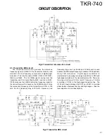
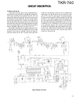
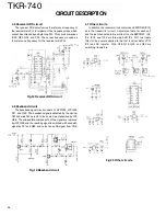
4.5 Receiver DDS circuit
The receiver DDS circuit varies the reference frequency of
the receiver main PLL to implement fine frequency steps which
cannot be achieved by a single-loop PLL. This circuit comprises
IC20, Q33, Q39, and CF5. The output frequency is used as
the reference frequency for the receiver main PLL.
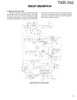
Fig.19 Baseband circuit
4.6 Baseband circuit
The baseband signal circuit consists of HPF Q26, LPF Q28,
D11, and Q29. The baseband signals detected by the narrow
FM and w ide FM detector circuits are de-emphasized by LPF
Q28. The sub-audible components of the signal are removed
by HPF Q26, and the resulting signal is switched with a squelch
signal by D11 and Q29, and output as an RA signal from CN6.
4.7 Other circuits
In addition, the receiver circuit contains an EEPROM (IC10)
as in the transmitter circuit. Adjustment data for each unit
and the last channel data are w ritten into the EEPROM . IC2,
IC4, IC13, and IC16 are three-pin AVR ICs. Q17 is a ripple
filter for the pow er supplied to the first local oscillator VCO.
IC3 is a shift register. Q16, Q18, Q19, Q20, and Q22 are
sw itching transistors.
Fig.18 Receiver DDS circuit
Fig.20 Other circuits
CIRCUIT DESCRIPTION
Summary of Contents for TKR-740
Page 97: ...TKR 740 TKR 740 BLOCKDIAGRAM 121 122 ...
Page 99: ...TKR 740 TKR 740 INTERCONNECTION DIAGRAM 125 126 ...
Page 101: ...MEMO 129 ...

