TKR-D710
14
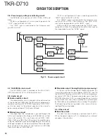
provides a second mixer, AGC amplifi er, and RSSI (Received
Signal Strength Indicator).
The second mixer mixes the fi rst IF signal with the 57.6
MHz of the second local oscillator output and produces the
second IF signal of 450kHz.
The second IF signal is passed through the ceramic fi lter
(CF401, CF402 and CF403) to reject the adjacent channel
signal. The fi ltered second IF signal is amplifi ed by the sec-
ond IF amplifi er (IC404) and AGC amplifi er (IC403).
The signal from the AGC amplifi er is input to the AD con-
verter (X53-458: IC20) through the ceramic fi lter (CF400) and
operational amplifi er (IC400 and X53-458: IC20).
2-8. Receiver PLL circuit (SUB unit)
■
VCO
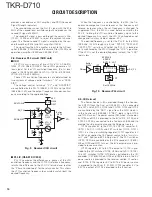
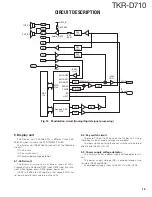
RX VCO circuit consists of two VCOs (VCO A X58-519:
Q352, VCO B X58-519: Q353). Those VCOs generate a 1st
local signal. For the VCO oscillation frequency, the 1st local
signal is 194.05 to 232.05MHz. (VCO A: 194.05~213.05MHz,
VCO B: 213.05~232.05MHz)
Those VCO oscillation frequencies are determined by
two systems of voltage control terminals: “CV” and “RXAS-
SIST”.
The voltage control terminals, “CV” and “RXASSIST”,
are controlled by the PLL IC (X58-519: IC300) and the MCU
(X53-458: IC20) and the output frequency changes continu-
ously according to the applied voltage.
D355
D352
D358
D359
SW
Q350
Q351
RXVCOA/B
RX_CV
RXASSIST
80C
VO
VCO_A
Q352
Buffer
Q354
D357
D353
D360
D361
VCO_B
Q353
Fig. 9 Receiver VCO circuit
■
PLL IC (X58-519: IC300)
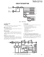
PLL IC compares the differences in phases of the VCO
oscillation frequency and the VCTCXO reference frequency,
returns the difference to the VCO CV terminal and realizes
the “Phase Locked Loop” for the return control. This allows
the VCO oscillation frequency to accurately match (lock) the
desired frequency.
When the frequency is controlled by the PLL, the fre-
quency convergence time increases as the frequency dif-
ference increases when the set frequency is changed. To
supplement this, the MCU is used before control by the
PLL IC to bring the VCO oscillation frequency close to the
desired frequency. As a result, the VCO CV voltage does not
change and is always stable at approx. 3.0V.
The desired frequency is set for the PLL IC by the MCU
(X53-458: IC20) through the 3-line “SPSD0”, “SPSCLK0”,
“/RXPCS_TR” serial bus. Whether the PLL IC is locked or
not is monitored by the MCU through the “LDR” signal line.
If the VCO is not the desired frequency (unlock), the “LDR”
logic is low.
Ref 19.2MHz
LDT
SPSCLK0
SPSD0
/RXPCS
Buffer
Q300
RX VCO/PLL
IC300
LPF
RX_CV
LPF
FIN
Loop filter
Fig. 10 Receiver PLL circuit
2-9. AVR circuit
The Power Source (+B) is provided through the Connec-
tor (CN701) from the Final unit (X45-401). +B is connected
to a FET switch (Q702, Q703) and CN700. Q702 and Q703
are controlled by the “SBC” signal from the MCU which is
in the Control unit (X53-458). If “SBC” logic is high, Q702
and Q703 turn on. The power source (SB) which is turned on
by Q702 and Q703 is provided to the 8V AVR IC (IC702) and
CN700. CN700 is connected to the Control unit (X53-458) to
provide the +B power source and the SB power source.
IC702 supplies 8V to the VCO, 15V DC/DC converter IC
(IC701), AVR IC (IC700) and FET switches (Q700, Q701).
IC701 is a step-up switching regulator. IC701 regulates 8V
to 15V and supplies the 15V power source to the “assist cir-
cuit” and “front-end BPF tuning circuit”. The FET switches
(Q700, Q701) are controlled by the I/O expander IC (IC805).
When Q700 and Q701 turn on, the 8V power source is pro-
vided to receiver section.
IC700 regulates 5V to 8V. The output of IC700 is pro-
vided to the FET switches (Q705, Q706) and AVR IC (IC703).
The FET switches (Q705, Q706) are controlled by the I/O
expander IC (IC805). When Q705 and Q706 turn on, the 5V
power source is provided to the receiver section, IF section
and IC704. IC704 regulates 5V to 3V. The 3V power source
is provided to the Mixer IC (IC300). IC703 regulates 5V to
3.3V. The output of IC703 is provided to the IF section.
CIRCUIT DESCRIPTION
Summary of Contents for TKR-D710
Page 71: ...TKR D710 71 MEMO ...
Page 108: ...TKR D710 108 MEMO ...
Page 110: ...Printed in Japan No RQ148 Communications Systems Business Operation ...


