TM-481A
8
Control Circuit
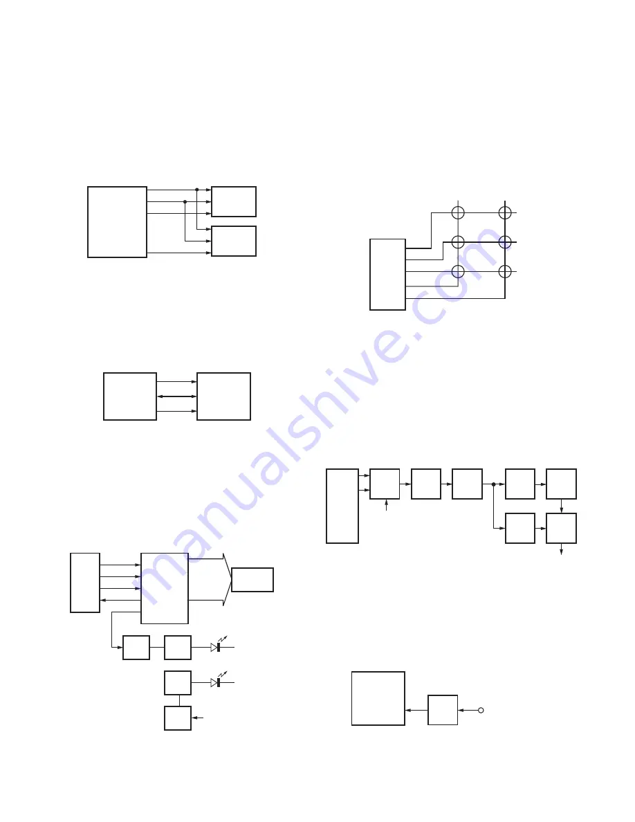
The MCU carries out the following tasks (See Fig. 10.):
1) Controls the WIDE, NARROW, and TX/RX outputs.
2) Controls the display circuit.
3) Controls the PLL IC (IC1).
4) Controls the D/A converter (IC705) and adjusts the vol-
ume, modulation and transmission power.
IC705
D/A
converter
IC1
PLL
IC707
MCU
EVLLD
DT
CK
PLLE
Fig. 10 Control circuit
■
Memory Circuit
The transceiver has an 64k-bit EEPROM (IC708). The
EEPROM contains adjustment data. The MCU (IC707) con-
trols the EEPROM through three serial data lines. (See Fig.
11.)
EEPCK
IC707
MCU
IC708
EEPROM
EEPSDT
EEPWP
Fig. 11 Memory circuit
■
Display Circuit
The MCU (IC707) controls the display LCD and LEDs.
When power is on, the LCD driver will use the BL line to
control the LCD illumination and key backlight LEDs.
The brightness function is controlled by switch Q
9
04. The
LCD driver (IC
9
01) and MCU (IC707) communicate through
the CE, CL, DI, and DO lines. (See Fig. 12.)
Q901
SW
Q902
SW
IC707
MCU
D903~D905
Q903
SW
D906~D911
Q904
SW
IC901
LCD
driver
CE
CL
DO
DI
BL
COM0~
COM3
SEG0~
SEG30
LCD
BRI
Fig. 12 Display circuit
■
Key Matrix Circuit
The front panel has function keys. Each of them is con-
nected to a cross point of a matrix of the KI1 to KI3 and KSI
to KS2 ports of the LCD driver.
The LCD driver monitors the status of the KI1 to KI3 and
KS1 to KS2 ports. If the state of one of the ports changes,
the LCD driver assumes that the key at the matrix point cor-
responding to that port has been pressed.
IC901
LCD
driver
KI1
KI2
KI3
KS2
KS1
FUNC
REV
CALL
VFO
MR
MHz
(Encoder)
Fig. 13 Key matrix circuit
■
Encode
The CTCSS and DCS signals are output from TONE of
the MCU (IC707). The DTMF signal is output from DTMF
of the MCU (IC707). These signals are summed with a MIC
signal by the summing amplifi er (IC706), and the resulting
signal goes to the D/A converter (IC705) to adjust the MOD
level, and then goes to the buffer amplifi er (IC706).
Part of the signal goes to the TCXO, and the rest goes to
the D/A converter (IC705) in order to adjust the modulation
balance between the VCO and TCXO.
X1
TCXO
VCO
IC706
SUM
AMP
IC705
D/A
IC705
D/A
IC706
BUFFER
IC1
PLL
Amp
MIC
IC707
MCU
TONE
DTMF
Fig. 14 Encode
■
Decode
• CTCSS/DCS
The signal (W/NO (EVOL2)) goes to DTMF IN (pin
9
5) of
the MCU (IC707) through the amplifi er (IC70
9
). The CTC-
SS/DCS signal will pass through the low-pass fi lters in the
MCU (IC707) and be decoded within the MCU (IC707).
IC707
MCU
IC709
AMP
DTMF IN
W/NO (EVOL2)
95
Fig. 15 Decode
CIRCUIT DESCRIPTION


