

DOT
DOT
DOT
DOT MATRIX
MATRIX
MATRIX
MATRIX
LIQUID
LIQUID
LIQUID
LIQUID CRYSTAL
CRYSTAL
CRYSTAL
CRYSTAL DISPLAY
DISPLAY
DISPLAY
DISPLAY
MODULE
MODULE
MODULE
MODULE
Serial
Serial
Serial
Serial
USER
USER
USER
USER‘‘‘‘ MANUAL
MANUAL
MANUAL
MANUAL
PROPOSED
PROPOSED
PROPOSED
PROPOSED BY
BY
BY
BY
APPROVED
APPROVED
APPROVED
APPROVED
Design
Approved
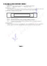
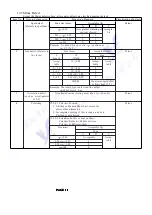
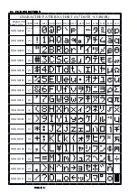
G16080-1


