FP520 Service Manual
Page 11 of 64
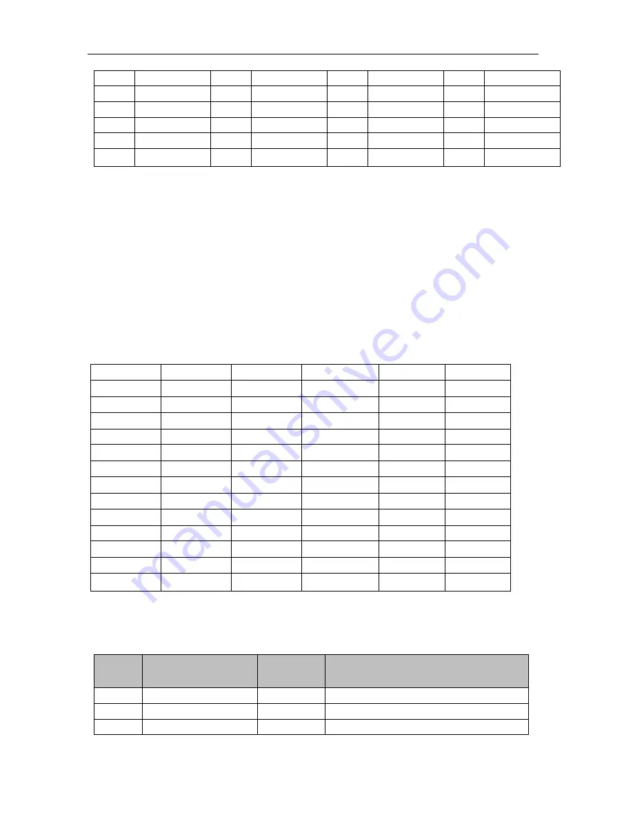
5
77.0
15
107.2
25
151.4
35
218.1
6
79.7
16
110.9
26
156.7
36
225.7
7
82.5
17
114.8
27
162.2
37
233.6
8
85.4
18
118.8
28
167.9
38
241.8
9
88.5
19
123.0
29
173.8
39
250.3
10
91.5
20
127.3
30
179.9
DCS Signaling:
DCS
(
Digital code squelch,
),
a continuous numerical code which is modulated along with the speech signal on the
carrier to control the squelch. If the DCS feature is set, the speaker is on only when the same DCS code is received
to avoid the unnecessary signal interference.
83 kinds of standard code of this radio are available. See chart 2.
DCS signal is generated by MCU (PWM wave form), and it is sent to VCO and TCXO for modulation after being
filtered by the low pass filter composed of RC for eliminating the frequency higher than 300Hz. VCO modulates the
high frequency of DCS signal and TCXO modulates the low frequency of DCS signal.
CTCSS/DCS signal from the receiver is sent to MCU for decoding. MCU identifies whether the receiving signal has
the same DCS code as the radio so as to turn on the speaker.
Chart 3.2 DCS Coding Chart
023
114
174
315
445
631
025
115
205
331
464
632
026
116
223
343
465
654
031
125
226
346
466
662
032
131
243
351
503
664
043
132
244
364
506
703
047
134
245
365
516
712
051
143
251
371
532
723
054
152
261
411
546
731
065
155
263
412
565
732
071
156
265
413
606
734
072
162
271
423
612
743
073
165
306
431
624
754
074
172
311
432
627
3.9 Semiconductor Device Description
MCU Description
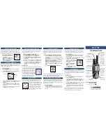
Chart 3.3 Microprocessor (M30620) Port Description
Pin No.
Port Name
Input/ output
Function
1
VCCN
D/A Output
TCXO tuned voltage output
2
TONE-OUT
D/A Output
TONE output
3
NC
I
NC
Summary of Contents for FP520
Page 1: ... 键入文档副标题 gh 选取日期 在此处键入文档的摘要 摘要通常是对文档内容的简短总结 在此处键入文档的摘要 摘要 通常是对文档内容的简短总结 ...
Page 44: ...FP520 Service Manual Page 43 of 64 Figure 1 FP520 01 Mainboard Schematic Diagram 136 174MHz ...
Page 45: ...FP520 Service Manual Page 44 of 64 ...
Page 46: ...FP520 Service Manual Page 45 of 64 ...
Page 47: ...FP520 Service Manual Page 46 of 64 ...
Page 48: ...FP520 Service Manual Page 47 of 64 ...
Page 49: ...FP520 Service Manual Page 48 of 64 ...
Page 50: ...FP520 Service Manual Page 49 of 64 ...
Page 51: ...FP520 Service Manual Page 50 of 64 ...
Page 54: ...FP520 Service Manual Page 53 of 64 Figure 4 FP520 02 Mainboard Schematic Diagram 400 470MHz ...
Page 55: ...FP520 Service Manual Page 54 of 64 ...
Page 56: ...FP520 Service Manual Page 55 of 64 ...
Page 57: ...FP520 Service Manual Page 56 of 64 ...
Page 58: ...FP520 Service Manual Page 57 of 64 ...
Page 59: ...FP520 Service Manual Page 58 of 64 ...
Page 60: ...FP520 Service Manual Page 59 of 64 ...
Page 61: ...FP520 Service Manual Page 60 of 64 ...
Page 64: ...FP520 Service Manual Page 63 of 64 Figure 7 KBC 51 7 4V Electrical Schematic Diagram ...


