FP520 Service Manual
Page 8 of 64
Fig.3.3 Diagram of Power Amplification and Antenna Switch Principle
The modulated RF signal from VCO, being amplified by Q303
、
Q304
、
Q602
、
Q603
、
Q601, is sent to Q600 for power
amplification.
The grid bias of Q601 and Q600 is controlled by APC (Automatic Power Control) circuit. Change the grid bias
voltage to easily control the output power strength of the transmitter.
APC
(
Automatic Power Control
)
Circuit
R620, R621 and R622 are power amplifier current detection, and IC600A is a power amplifier current sampling
amplifier. IC600B is a power comparison amplifier.
The extra high output power of the transmitter will increase the power amplifier current and IC600A output with a
decrease in IC600B output voltage. It will also decrease the bias voltage on Q601 and Q600, which decreases the
output power of the transmitter, and vice versa. This enables the stability of the output power in different working
circumstances.
MCU changes the voltage being sent to IC600B to set the power.
3.5 Principle of Frequency Synthesizer
PLL
DATA
Q301
RF AMP
LPF
Q302
RX VCO
PLL
DATA
Q303
BUFF AMP
12.8MHz
TCXO
X300
IC300
PLL IC
Q307
TX VCO
Q305,Q306
SW
Q304
RF AMP
MCU
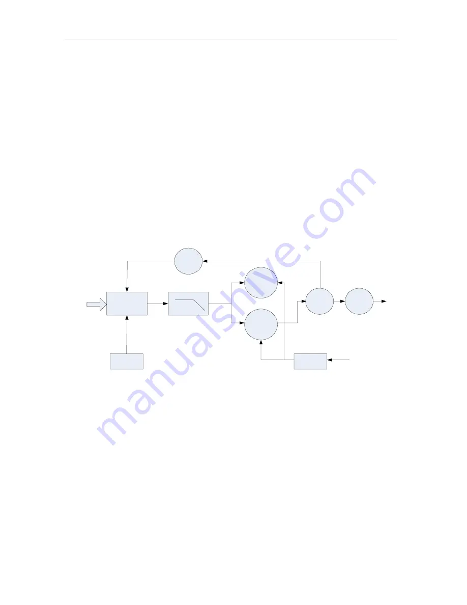
Fig 3.4 Diagram of Frequency Synthesizer
This radio applies PLL frequency synthesizer.
The frequency synthesizer consists of reference oscillator, voltage controlled oscillator (VCO), programmable
frequency divider, phase comparator and low pass filter.
Q307, D305, D306, D307, D308 and other resistance-capacitance units make up the transmitting VCO unit. D304 is
the modulation circuit of the transmitting VCO.
Q302
、
D300
、
D301
、
D302
、
D303 and other resistance-capacitance units make up the receiving VCO unit.
IC300 (MB15E03) is a PLL integrated circuit which contains a programmable reference frequency divider,
programmable frequency divider, phase comparator and charge pump.
R329, C358, R330, C359, R331, R332 and C360 make up the loop filter.
The reference frequency is provided by X300 (TCXO
,
12.8MHz).
The reference frequency from TCXO (Temperature Controlled Crystal Oscillator
)
is divided by the programmable
reference frequency divider in IC300 to become the 5kHz or 6.25kHz (controlled by MCU, according to the setting
channel) reference frequency .
The oscillation frequency from VCO, being amplified by the two-time frequency multiplier circuit, is sent to IC300 for
Summary of Contents for FP520
Page 1: ... 键入文档副标题 gh 选取日期 在此处键入文档的摘要 摘要通常是对文档内容的简短总结 在此处键入文档的摘要 摘要 通常是对文档内容的简短总结 ...
Page 44: ...FP520 Service Manual Page 43 of 64 Figure 1 FP520 01 Mainboard Schematic Diagram 136 174MHz ...
Page 45: ...FP520 Service Manual Page 44 of 64 ...
Page 46: ...FP520 Service Manual Page 45 of 64 ...
Page 47: ...FP520 Service Manual Page 46 of 64 ...
Page 48: ...FP520 Service Manual Page 47 of 64 ...
Page 49: ...FP520 Service Manual Page 48 of 64 ...
Page 50: ...FP520 Service Manual Page 49 of 64 ...
Page 51: ...FP520 Service Manual Page 50 of 64 ...
Page 54: ...FP520 Service Manual Page 53 of 64 Figure 4 FP520 02 Mainboard Schematic Diagram 400 470MHz ...
Page 55: ...FP520 Service Manual Page 54 of 64 ...
Page 56: ...FP520 Service Manual Page 55 of 64 ...
Page 57: ...FP520 Service Manual Page 56 of 64 ...
Page 58: ...FP520 Service Manual Page 57 of 64 ...
Page 59: ...FP520 Service Manual Page 58 of 64 ...
Page 60: ...FP520 Service Manual Page 59 of 64 ...
Page 61: ...FP520 Service Manual Page 60 of 64 ...
Page 64: ...FP520 Service Manual Page 63 of 64 Figure 7 KBC 51 7 4V Electrical Schematic Diagram ...


