background image

3


Top Button

Programmable  function  button:  Press  it  to  activate  the 

programmable auxiliary function. 

 Microphone/Speaker Jacks

For connecting the optional Microphone/Speaker.


      Chapter 3 Electrocircuit

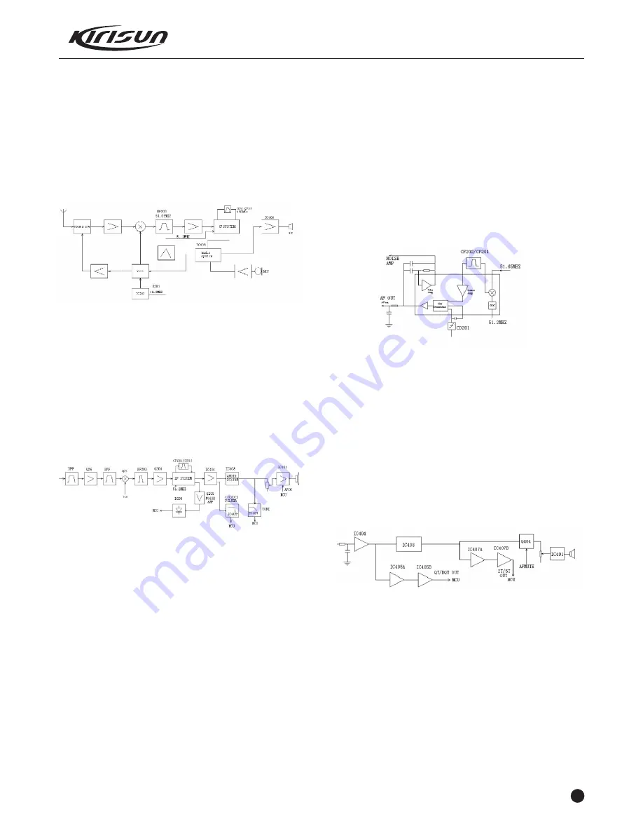
3.1 Frequency Configuration  

                     Figure 3.3 Frequency Configuration

This  radio  adopts  the  2nd  Mixer,  the  1st  IF  51.65MHz,  the  2nd  IF 

450kHz.

The  receiver's  first  local  oscillation  is  generated  by  the  frequency 

synthesizer.  The  second  local  oscillation  adopts  the  4th  harmonic 

51.2MHZ of TCXO.

The transmitter signals are generated by frequency synthesizer.

The  reference  frequency  of  frequency  synthesizer  is  generated  by 

TCXO.

3.2 Receiver (RX)

                           Figure 3.4 Receiver (RX)

The Receiver Front Terminal   

Signals  from  the  antenna  pass  through  the  RX/TX  switch  (D102, 

D103,  D104);  and  then  undesirable  out-of-band  signals  will  be 

filtered  out  at  the  band  pass  filter  (BPF)  consisting  of  C260,  L756, 

L732,  C259,  C750,C731,D700,C730,L212,C256

C257

D210

C255

L211

C253

and  D209;  then  signals  are  amplified  at  the 

low  noise  amplifier  (LNA)  consisting  of  Q26  and  its  peripheral 

components. 

The  output  from  the  LNA  passes  the  BPF  consisting  of  L207

L206

L720

C248

C702

D207

C245

C244

and  C733  for 

filtering and then is sent to the first grade frequency mixer (Q21).

The First Frequency Mixer

After  mixing  the  receiving  signals  from  LNA  with  the  first  local 

oscillation signals from the frequency synthesizer, the 1st IF signals 

51.65MHz

are  generated.  The  first  IF  signals  pass  the  crystal 

filter  (XF203),  which  will  filter  the  signals  of  adjacent  channel  and 

those out of band. 

IF Circuit

The 1st IF signals from the crystal filter are amplified at the first IF 

amplifier (Q204), and then are sent to the IF processing IC (IC204, 

TA31136FN). 

The  IF  IC  consists  of  the  2nd  frequency  mixer,  the  2nd  local 

oscillator,  IF  amplifier,  limiter,  phase  frequency  detector,  and  noise 

amplifier.

After amplifying TCXO (X301),  the  4th  harmonic  51.2MHz  is  made 

as the signal source of the 2nd local oscillation. The 2nd oscillation 

signal

51.2MHz

and the 1st IF signal

51.65MHz

are mixed at 

IC204  to  generate  2nd  IF

450kHz

.  After  the  2nd  IF  signal  is 

amplified  and  its  amplitude  is  limited  at  IC204,  and  then  filtered  at 

porcelain  filter  (wide  band  CF201/  narrow  band  CF202

450kHz), 

IC204 demodulates and sends out audio signals.

                                         Figure 3.5 IF System 

Receiver Audio Signal Processing

IC404

IC405

IC407

and  IC408  and  their  peripheral  circuit 

compose  the  receiver  audio  signal  processing  circuit.  IC204  sends 

audio signals to IC404 for amplification, and then one route goes to 

IC405 (CTCSS signaling filtering circuit) for waveform shaping and 

then  to  IC6-D;  one  route  goes  to  IC408  where  the  signals  are 

amplified, de-emphasized, filtered and the HF (high frequency) and 

LF  (low  frequency)  will  be  eliminated,  and  then  for  the  remaining 

300-3000Hz  audio,  one  route  is  sent  to  volume  potentiometer  for 

adjustment  and  finally  sent  to  the  audio  amplifier  (IC401),  and  the 

other one route passes IC407 (2-Tone/5-Tone filter ) to MCU.

               Figure 3.6 Receiver Audio Signal Processing

Squelch Circuit

Demodulation output from IC204 is sent to the selection frequency 

noise  amplifier,  which  consists  of  IC204  inner  noise  amplifier  and 

C121

R252

R211

C209

and R212 to be filtered off the noise. 

After  being  amplified  at  Q205,  noise  is  sent  to  D299  for  wave 

checking  and  then  sent  to  MCU,  which  determines  the  noise 

volume to control the squelch.

Audio Amplifier

IC401  and  its  peripheral  components  construct  the  BTL  audio 

amplifier.

Receiving  audio  signals,  voice  indication  signals,  indication  tone 

signals  and  warning  tone  signals  are  collected  for  audio 

amplification  to  drive  the  speaker.  Warning  tone  has  no  volume 

PT5200 SERVICE MANUAL

Summary of Contents for PT5200-01

Page 1: ...PROFESSIONAL TWO WAY RADIO PT5200 V070607 FM P RTABLE RADIO SERVICE MANUAL O ...

Page 2: ...he MCU software Kirisun Electronic Shenzhen Co Ltd owns the copyright of the radio outward structure circuit design Kirisun Electronic Shenzhen Co Ltd owns the copyright of this service manual Unauthorized publication is prohibited Kirisun Electronic Shenzhen Co Ltd owns the trademarks KIRISUN 科立讯 CONTENTS Chapter 1 Introduction Chapter 2 Radio Overview and Function Keys 2 Chapter 3 Electrocircuit...

Page 3: ...fill in a component application forms if you want to apply for any components from Kirisun The following is one sample form that might be used to apply for any components from Kirisun Component Application Compo Radio Model Material Serial No No pecifications nent S Model PT5200 01 FET Q104 RD07MVS1 105 RD07MV 001 1 PT5200 01 Triode Q101 2SC5108 Y 104 SC5108 001 1 Qua ntity 1 3 Service All the Kir...

Page 4: ...he 2nd frequency mixer the 2nd local oscillator IF amplifier limiter phase frequency detector and noise amplifier After amplifying TCXO X301 the 4th harmonic 51 2MHz is made as the signal source of the 2nd local oscillation The 2nd oscillation signal 51 2MHz and the 1st IF signal 51 65MHz are mixed at IC204 to generate 2nd IF 450kHz After the 2nd IF signal is amplified and its amplitude is limited...

Page 5: ...o Q11 and Q12 will decrease and then the transmitter output power will decrease Vice versa such can ensure steady transmitter output power in different working circumstances MCU changes the input power to IC3B to set the power Transmitter Audio Signal Processing Figure 3 9 Transmitter Audio Circuit IC402 and IC408 and their peripherals components construct the transmitter audio processing circuit ...

Page 6: ... Figure 3 11 MCU Diagram MCU controls the working of each location of the radio to realize all the radio functions Connects with the PC Accesses the radio status data Controls PLL to generate the receiving and transmitting local oscillation frequency Accesses the current channel status Controls the LED status indication Controls the power supply of each location Checks the action of each function ...

Page 7: ... RX audio mute control output H audio output L mute Frequency shift selection control Control Power Save mode output To select the width of the external data bus high level is 8 digit width working mode switching control Backup clock input Backup clock output Reset input Clock output Ground Clock input Power positive polarity input AK2346 RDF input AK2346 TATA output AK2346 MSK clock 19 20 21 22 2...

Page 8: ...nal power amplifier Transmitter power amplifier drive APC output switch The 1st frequency mixer Receiver HF amplifier The 1st IF amplifier Red LED drive Green LED drive Table 3 5 Diode Function Description Position D102 D101 D103 D104 D201 D302 D304 D305 D310 D308 ZD101 D311 D306 D299 D508 D509 D505 D506 Type MA77 HSC277 HSC277 HSC277 HSC277 MA2S376 MA2S376 MA360 MA2S376 MA2S376 HZU5ALL MA2S111 MA...

Page 9: ...hannel even the normal channel is receiving signals at that time And the radio will stay on the priority channel till that signal disappears The dealer can set the delay time between signal disappearing and continuing scanning d Temporarily Delete When scanning pauses on a channel channel press and hold the button programmed as Temporarily Delete or Scan Temporarily Delete for 1 second to delete t...

Page 10: ...d you can transmit on the busy channel 2 Carrier wave If carrier wave is detected the radio is unable to transmit 3 CTCSS DCS The radio is allowed to transmit when the CTCSS DCS signalings are identical 4 Selective signaling The radio is allowed to transmit when the selective signalings 2 Tone or 5 Tone are identical 4 1 12 Squelch Level Selection The purpose of the squelch is to mute the speaker ...

Page 11: ...perating steps are as follows 1 Turn on the radio with the MONI key pressed and 2 seconds later the red light flashes twice and two beep tones sound and then the radio enters the wired clone mode 2 Press the PTT button on the host radio to activate inactivate the wired clone mode on the sub radio But the wired clone mode of the host radio will not be changed When pressing the PTT button the green ...

Page 12: ... 2 1 1 2 1 2 2 2 1 1 1 1 1 3 1 10 1 32 33 34 35 36 24 25 26 27 28 29 30 31 2 204 000558 R04 204 003208 R05 202 000558 R06 201 000558 R07 202 000558 R08 203 003208 R02 302 17040G R01 202 003208 R07 202 000558 R07 203 000558 R07 204 000558 R05 203 004200 R01 203 003208 R04 2 1 1 2 1 1 1 1 1 1 1 1 PTT COVER BOARD PTT PLASTIC KEYSTROKE PTT KEYSTROKE SPEAKER SPRING LOGO LABLE SURFACE SHELL SPEAKER LIGH...

Page 13: ...2 1 1 1 1 1 1 1 1 2 2 2 1 1 1 1 10 1 2 1 2 1 1 121 100000 R07 201 000558 R08 201 000558 R09 201 005200 R02 202 000558 R03 204 000558 R01 204 006800 R06 201 000668 R03 203 003208 R09 201 000558 R07 202 000558 R06 202 000558 R08 203 003208 R02 302 17040G R01 202 000558 R08 203 003208 R04 203 004200 R01 204 000558 R02 204 000558 R03 204 000558 R05 301 20030G R03 201 000558 R05 202 000558 R14 203 0005...

Page 14: ...nce the radio needs to be tested and debugged after replacing components Some certain radio parameters can be modified computer mode with our KSP 5200 programming software The modifiable parameters are as follows 1 Frequency difference 2 TX power 3 Low battery power warning threshold 4 Squelch level 5 CTCSS QT frequency deviation 6 DCS DQT frequency deviation 7 TX frequency deviation 8 DTMF freque...

Page 15: ...keyboard to enter DTMF Frequency Deviation Narrow Band and press Enter Press key to make the DTMF Frequency Deviation at 1 5 0 1KHZ 6 3 9 TONE Frequency Deviation Adjustment Under the computer test mode press on the keyboard to enter TONE Frequency Deviation Wide Band and press Enter Press key to make the TONE Frequency Deviation at 3 0 3KHZ Press on the keyboard to enter TONE Frequency Deviation ...

Page 16: ...ation Frequency Deviation Modulation Sensitivity Modulation Distortion 300 3000Hz Adjacent Channel RF Power Spurious and Harmonics Residential Frequency Modulation Transmitting Current Sinking 4 0W 7 5V DC 6 2 5 10 5kHz 15mV 3 70dB 70 dB 45 dB 1 8A 7 5V DC Chapter 8 Trouble Shooting No display after switching on the radio PLL is unlocked Beep sounds Cannot talk to or hear other group members Canno...

Page 17: ...s filter MCU micro control unit MIC microphone MOD modulation MONI monitor PLL phase lock loop PTT push to talk RX receiver SPK speaker TCXO temperature compensated crystal oscillators TX transmitter UL un lock VCO voltage control oscillator Appendix 2 Framework Component List 1 2 3 4 5 6 7 8 9 10 11 12 13 14 15 16 17 18 19 201 005200 R04 201 000668 R02 201 000668 R03 201 000668 R04 201 000668 R05...

Page 18: ... R01 102 DA2822 R01 102 FP3502 R01 102 K11250 R01 102 M2904V R01 102 M30620 R01 102 P502PR R01 102 T24C64 R01 103 00MA77 R01 103 0MA742 R01 103 1SR154 R01 103 1SS373 R01 103 1SV278 R01 103 A2S077 R01 103 A2S111 R01 103 DAN222 R01 103 HVC350 R01 103 HVC376 R01 103 L190YG R01 103 MHC190 R02 103 RB706F R01 103 Z80680 R01 104 00UMC4 R01 104 A144EE R01 104 C114EE R01 104 C144EE R01 104 SA1745 R01 104 S...

Page 19: ...stor 0402 18K 5 Chip resistor 0402 180K 1 Chip resistor 0402 1 8M 5 Chip resistor 0402 2K 5 Chip resistor 0402 20K 5 Chip resistor 0402 200K 5 Chip resistor 0402 22R 5 Chip resistor 0402 220R 5 Chip resistor 0402 2 2K 5 Chip resistor 0402 22K 5 Chip resistor 0402 220K 5 Chip resistor 0402 270R 5 Chip resistor 0402 27K 5 Chip resistor 0402 300R 5 Chip resistor 0402 30K 5 Chip resistor 0402 300K 5 C...

Page 20: ... 25V X7R Chip capacitor 0402 1P 0 25P 50V C0G Chip capacitor 0402 1 5P 0 25P 50V C0G Chip capacitor 0402 20P 5 50V C0G Chip capacitor 0402 22P 5 50V C0G Chip capacitor 0402 220P 5 50V C0G Chip capacitor 0402 2200P 10 50V X7R Chip capacitor 0402 0 022uF 10 50V X7R Chip capacitor 0402 0 22uF 10 16V X7R Chip capacitor 0402 27P 5 50V C0G Chip capacitor 0402 0 027uF 10 50V X7R Chip capacitor 0402 2P 0 ...

Page 21: ...Model SIZE P 10uF 20 6 3V Chip Ta capacitor TPModel SIZE P 4 7uF 20 10V Chip capacitor 0805 1uF 80 20 16V Y5V Chip capacitor 0805 2 2uF 80 20 10V Y5V Chip Ta capacitor TS Model SIZE A 1uF 20 10V Chip Ta capacitor TS Model SIZE A 10uF 20 16V Chip Ta capacitor TS Model SIZE A 2 2uF 20 10V Chip Ta capacitor TS Model SIZE A 0 33uF 20 35V Chip capacitor 1206 0 1uF 10 50V X7R Chip Ta capacitor TS Model ...

Page 22: ...3M686 R01 124 050000 R04 124 050000 R05 125 041022 R01 125 041024 R01 603 0W558A R01 Hot quick resistor NTH5G16P40B473J 47K 5 0603 Mic socket B6027AP402 88 old Model B6027AP402 65 Chip transistor 10MHz CSTCC10 0MG TC 3 7mm Chip transistor 12 8MHz TCXO DSA535SA Plug in crystal oscillator 3 6864MHz 3 5mm Mic socket SP MIC ST 212 2 5mm Eearphone socket SP MIC EJ 2507 CCPA Chip net resistor 1K 2 0402 ...

Page 23: ......

Page 24: ......

Page 25: ... NC R432 100k R459 4 7k C461 0 01u C460 5600p C463 0 1u R463 10k R465 150k C465 0 1u C464 4 7u 6 3v R461 10k R462 1m R464 150k R466 1k R467 10k C497 1000p R429 100k R430 100k R433 22k R452 18k R451 18k C450 0 01u C452 4 7u 6 3v R449 390k C451 220p R450 82k R448 100k C449 0 039u D410 MA742 C448 103 R447 180k R446 180k R445 22k C446 0 068u C447 2200p R5V C459 0 1u R431 22k C456 0 1u C490 0 1u C410 0...

Page 26: ...25 Figure4 PT5200 Schematic Circuit Pane Diagram PT5200 SERVICE MANUAL ...

Page 27: ...Figure 5 KBC 42A Schematic Circuit Diagram PT5200 SERVICE MANUAL 26 ...

Reviews: