PT568 Service Manual
4
Audio signal processing
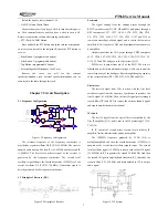
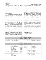
The voice signal processing circuit of the receiver consists of
IC6 and its peripheral circuits. After being amplified in IC6-C,
voice signal from IC5 is sent to IC4 (CTCSS signal filtering
circuit) and IC6-D respectively. The signal is then amplified,
deemphasized and filtered by other units of IC6 to remove HF and
LF components contained in the audio frequency, with only voice
components within 300~3000Hz left. The resulting signal is then
sent to Q9 for amplification. The amplified signal is adjusted by
the volume potentiometer and then is sent to the audio power
amplifier (IC8).
Figure 3.4 Audio Processing of Receiver
Squelch circuit
The demodulated signal from IC5 goes to the selective noise
amplifier consists of internal noise amplifier of IC5, C211, R99,
R100, C107 and R94 to remove the noise component. The
resulting signal is then amplified by Q7 and demodulated by D17
and is sent to the MCU. MCU identifies level of the noise and
controls the squelch.
Audio power amplifier
The audio power amplifier circuit consists of IC8 and its
peripheral components.
The received audio signal, voice alert signal, alert tone signal
and warning tone signal are collected and pass through the audio
amplifier where they are amplified and output to drive the speaker.
The volume of the warning tone is not controlled by the preset
volume level of the radio.
When AFCO is in high level, Q35 turns on, IC8 starts to
operate, and the speaker makes sound. Speaker impedance: 16
Ω
.
Q38: Receiving audio signal switch
Q51: Warning tone switch
Q25: Alert tone switch
CTCSS/DCS signal filtering
Audio signal demodulated by IC5 may contain CTCSS
(Continuous Tone Control Squelch System) or DCS (Digital Code
Squelch) signal. The spectrum components of CTCSS/DCS are
within 2-250Hz. The filtering circuit consists of IC4 can remove
signals outside the CTCSS/DCS spectrum, which enables the
MCU to decode CTCSS/DCS more accurately.
3.3 Principle of Transmitter (TX)
TX power amplification
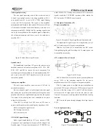
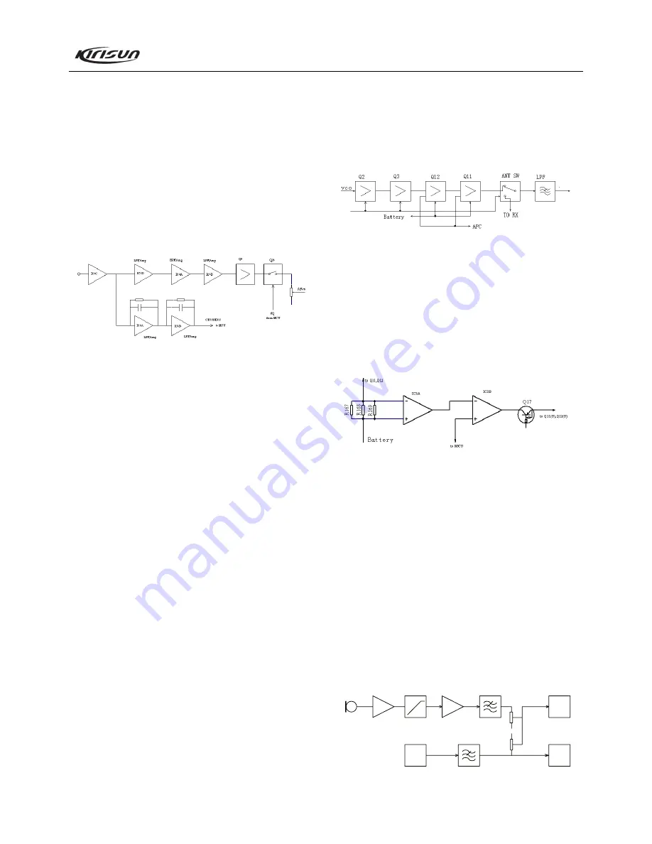
Figure 3.5 Principle of Power Amplifier and Antenna Switch
The modulated RF signal from VCO is amplified by Q2, Q3
and Q12, and is sent to Q11 for power amplification.
Grid bias of Q11 and Q12 is controlled by the APC circuit.
Through changing the grid bias voltage, the Tx output power can
be controlled conveniently.
APC (Automatic Power Control)
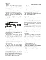
Figure 3.6 APC Circuit
R167, R168 and R169 are used to test the power amplification
current. IC3A is the sampling amplifier for the power
amplification current. IC3B is the power comparator amplifier.
If the Tx output power is too high, the power amplification
current and IC3A output will increase; IC3B output voltage will
decrease, so the bias voltage of Q11 and Q12 will also decrease,
which causes the Tx output power to be lowered, and vice versa.
Thus the Tx output power can keep stable under different working
conditions.
MCU can set the power through changing the voltage input to
IC3B.
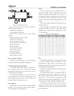
Tx voice signal processing
TCXO
VCO
MCU
CTCSS/DCS
MIC
MIC Amp
Pre-Emphasis
IC7A
IC7B
IC7C,IC7D
Figure 3.7 Transmitter Audio Circuit


