4
comparator, and the upper limiting filter.
Q6, D2, D4, D5 and D6 constitute the transmitting VCO unit. D9 is
the modulating circuit of the transmitting VCO.
Q11, D11, D12, D13 and D14 etc. constitute the receiving VCO
unit.
IC2 (ADF4111) is the PLL integrated circuit, which can comprise
the programmable reference frequency divider, programmable
frequency divider, phase comparator and charge pump, etc.
The upper limiting filter consists of R43 and C96 etc.
The frequency reference is provided by X1 (TCXO, 12.8MHz).
The frequency reference from TCXO (temperature control crystal
oscillator) receives frequency division by the programmable
reference frequency divider in IC2 to generate the frequency
reference of 5kHz or 6.25kHz (according to the frequency of the
channel, controlled by MCU).
The oscillation frequency from VCO is sent to IC2, after frequency
division by the programmable frequency divider, it is compared
with the frequency reference to get the error signal, which is, after
wave filtering by the upper limiting filter, sent to VCO to change
the oscillation frequency of VCO, which allows the VCO frequency
to achieve the set value and the VCO to be locked.Detection of
loss of lock: if PLL loses lock, IC2 pin14 outputs low level signal to
MCU, which prevents the transmitter from transmitting and
generates alert.
Q13 and related circuits are used for switching the upper limiting
filter.
3.5 Audio Processing Circuit:
I
C6 (AK2346) is a special voice processing chip provided with
functions like amplification, wave filtering, preemphasis,
deemphasis, scrambling, companding and MSK MODEM etc. Most
voice processing tasks of the radio are completed by it.
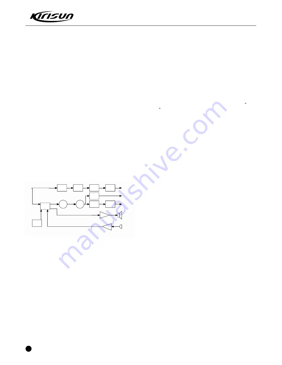
MIC Signal Processing:
Voice signals from MIC are controlled by AGC circuit, and then
reach IC24, one group of signals are amplified at IC24B (VOX
circuit) and are processed into direct current by D35 and sent to
MCU for processing; the other group of circuits are amplified at
IC24A and then receive amplification, wave filtering, companding
(optional), preemphasis, scrambling and amplitude limit at IC6 pin3,
after that, they are exported from IC6 pin7 and sent along with
CTCSS/DCS to VCO for modulation.
2T/5T signals are imported from IC6 pin6, and after amplitude limit
and amplification, they are exported form IC6 pin7 and sent to VCO
for modulation.
Receiver Audio Signal Processing:
Voice signals exported from IC4 are divided into two channels, one
comes to the low pass circuit (voice signals filtered) consisting of
IC5, etc for amplification and wave filtering to get comparatively
pure CTCSS/DCS signals, which are then sent to MCU for
processing; the other comes to IC6 pin23, after amplification and
wave filtering, one channel is exported from IC6 pin21 (DTMF/2T/5T
signals etc.), DTMF/2T/5T signals etc. come through the high pass
circuit (sub-audio signals filtered) consisting of Q30 and Q31 etc.,
DTMF signals come to IC10 (special chip for HT9172 DTMF
decoding) for decoding and then sent to MCU for processing, 2T/5T
signals are sent to MCU for processing after wave filtering and
waveform modification by IC1; the other channel of signals (voice
signals) are exported form IC6 pin18 after scrambling, preemphasis,
deemphasis and companding and then imported from IC6 pin19 for
amortizing and amplification before being exported form IC6 pin20.
IC13 is a voice storage chip, which stores voices including channel
prompt etc., each time the channel is changed, the speaker will
prompt the current channel number by voice. Press the
voice
prompt
key to prompt the current channel number again.
Receiver audio signals, voice prompt signals, 2T/5T/DTMF signals,
prompt voice signals, emergent alert signals are gathered to be
amplified by the audio frequency amplifier IC9 to drive the speaker.
Speaker impedance: 16Ù.
Note: None of the terminals of the speaker can be grounded!
The volume of emergent alerts cannot be controlled.
3.6 Power Supply:
The radio is equipped with 7.4V battery as power supply, which
directly supply power to transmitter power amplifier circuits (Q1, Q3)
and receiver audio power amplifier (IC9), other circuits adopts
regulated 5V power supply.
Q40, Q45: 5V low voltage difference, micro power regulator.
Q43: 5T switch, controlled by MCU.
5T: Supplies power for the front terminal of the transmitter.
Q39: 5R switch, controlled by MCU.
5R: Supplies power for the receiver RF amplification, mixing, IF
processing, audio signal processing..
Q44: 5C switch, controlled by MCU.
5C: Th e 5V power controlled by power saving supplies power for
the frequency synthesizer.
3.7 MCU:
MCU controls the working of each unit of the radio to realize
all the radio functions.
Connects with the PC
Accesses the current channel status data
Controls the PLL to generate receiver and transmitting local
oscillation frequency
Acquires current channel status
Controls the LED status indication
Controls the power supply of each location
Checks the action of each function key
Generates CTCSS signals
Generates DCS signals
Generates power control signals
CTCSS decoding
DCS decoding
Squelch check and control
Controls the content of voice indication
Memorizes the radio channel data, CTCSS/DCS data, and other
data of function setting and parameter adjustment.
CTCSS/DCS Encoding and Decoding:
2
Memorier (E PROM, AT24C256)
PT6500 SERVICE MANUAL
1
1
2
2
3
3
4
4
D
D
C
C
B
B
A
A
Titl e
Number
Revision
Size
A4
Date:
2007-7-26
Sheet of
Fil e:
X:\ PT6500\..\ AUDI O.SchDoc
Drawn By:
pin 7
Q30
HP
Q31
HP
IC1A
HP
AMP
IC1B
IC10
HT9172
IC5A
IC5B
IC5C
IC5D
AMP
LP
LP
AMP
CTCSS/ DCS
DTMF
2T
AK2346
IC6
IC4 pi n 9
AF AMP
IC9 TDA 8541
pin 20
MIC AMP
MCU
IC7
pin 23
pi
n
6
pi
n
3
MIC
SP
Figure 3.5 Audio Processing Diagram
Summary of Contents for PT6500
Page 1: ...PROFESSIONAL TWO WAY RADIO PT6500 V071208 FM PORTABLE RADIO SERVICE MANOAL Welcome ...
Page 33: ...PT6500 SERVICE MANUAL Figure 1 PT6500 Top Main Board Position Number Diagram 136 174MHz 32 ...
Page 34: ...PT6500 SERVICE MANUAL Figure2 PT6500 Bottom Main Board Position Number Diagram 136 174MHz 33 ...
Page 35: ...Figure 3 400 470MHz PT6500 Top Main Board Position Number Diagram 34 PT6500 SERVICE MANUAL ...
Page 36: ...35 PT6500 SERVICE MANUAL Figure 4 400 470MHz PT6500 Bottom Main Board Position Number Diagram ...
Page 37: ...Figure 5 PT6500 PTT Top Board Position Number Diagram 36 PT6500 SERVICE MANUAL ...
Page 38: ...37 PT6500 SERVICE MANUAL Figure 6 PT6500 PTT BOTTOM Board Position Number Diagram ...


