background image


PT6800 Service Manual


16

6) Tx deviation: nominal frequency


± 500Hz 

7) DTMF deviation: 3 – 4kHz (wideband)/1.5 – 2.0kHz 

(narrowband) 

8) FFSK deviation: 3 – 4kHz (wideband)/1.5 – 2.0kHz 

(narrowband) 

9) Battery low voltage indication: When the voltage is 6.6V, the 

LED blinks red while pressing PTT button, and the radio has no 

Tx power.   


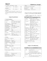
Chapter 8 Specifications 


8.1 General Specifications 

Product Model 

PT6800 

(136 ~ 174) MHz 

(400 ~ 470) MHz 

Frequency 

(470~ 520) MHz 

(350 ~ 390) MHz 

Type of Modulation   

16K

Ф

F3E/11K

Ф

F3E 

Number of Control Channel  6*64 

Channel Spacing 

25kHz/12.5kHz 

Intermediate Frequency 

1

st

 IF: 51.65MHz, 2

nd

 IF: 450kHz 

Operating Voltage 

7.5V, cathode grounded 

Operating Temperature 

-25

~ +55


Antenna Impedance 

50


MIC Impedance 

2.2k 


Battery (Standard 

Configuration) 

Model: KB-36C, Li-ion Battery: DC 

7.4V, 1750mAh, using time: 8h (cycle: 

5: 5: 90) 

Dimension (W×H×D) 

56mm × 120mm × 35mm 

Weight 

413g (with battery and antenna) 


8.2 Rx Part 

Usable Sensitivity (12dB 

SINAD) 

0.25

μ

Squelch ON Sensitivity 

0.185

μ

Rx Residual Output   

-40dB/

-35dB 

Rx Modulation Bandwidth 

±7kHz/±3.5kHz 

Adjacent Channel 

Selectivity 

70dB/

60dB 

Intermodulation Rejection 

60dB 

Spurious Response 

Rejection 

70dB 

Audio Output Power 

1.5W, balanced @ distortion 

 10%, 

16


Rx Current Consumption 

400mA 


8.3 Tx Part 

Tx Power 

4.0W/0.5W @ 7.5V DC 

Frequency Stability 

±2.5ppm 

Max. Modulation Deviation  ±5kHz/±2.5kHz 

Modulation Distortion (300 

3% 

~ 3000Hz) 

Adjacent Channel Tx Power

70dB/

60dB 

Spurious Emission 

70dB 

Residual FM 

45dB 

Tx Current Consumption 

1.7A @ 7.5V DC 


Chapter 9 Servicing and Testing Equipment 


Equipment and apparatus listed below are required for 

servicing and test of PT6800. 

No.

Name 

Major Specifications 

1

Standard signal 

generator 

Frequency range: 350 ~ 390MHz 

Modulation: FM and external modulation 

Output: -127dBm/0.1

μ

V ~


> -47dBm/1mV 

2

Power meter 

Input impedance: 50 


Operating frequency: 350 ~ 390MHz 

Measuring range: around 10W 

3 Deviation meter 

Frequency range: 350 ~ 390MHz 

4

Digital voltmeter 

Measuring range: DC 10mV ~ 10V 

Input impedance: High input impedance of 

min. circuit load 

5 Oscilloscope 

DC ~ 30MHz 

6

High sensitivity 

frequency counter

Frequency range: 50Hz ~ 10kHz 

Frequency stability: 0.2ppm or lower 

7 Ammeter 5A 

8

Audio frequency 

voltmeter 

Frequency range: 50Hz ~ 10kHz 

Voltage range: 1mV ~ 10V 

9

Audio frequency 

generator 

Frequency range: 50Hz ~ 5kHz or higher 

Output: 0 ~ 1V 

10

Distortion tester 

Capacity: 3% or lower @ 1kHz 

Input level: 50mV ~ 10vms 

11 Spectrum analyzer Measuring range: DC ~ 1GHz or higher 

12

Path generator 

Center frequency: 50kHz ~ 600MHz 

Output voltage: 100mV or higher 

13 16 

 dummy load

Around 16 

, 3W 

14

Adjustable power 

supply 

5V ~ 10V, around 5A 


Chapter 10 Troubleshooting 


No.

Problem 

Causes and Solutions 

1

Power ON 

failure 

A. The battery pack may be out of power. Please charge 

it or change a new one.   

B. Power switch in failure; please change it. 

C. CPU is broken, please change the IC. 

D. Zener diode Q45 is broken; please change the IC. 

2

PLL unlocked 

(Beeping) 

A. The PLL crystal oscillator X1 is broken. Please 

change it.   

B. The oscillator transistor is broken. Please change it. 

C. The PLL IC2 is broken. Please change it.   

Summary of Contents for PT6800

Page 1: ...rnal View and Functional Keys 1 Chapter 3 Mode Introduction 2 Chapter 4 Circuit Description 3 Chapter 5 Function Description and Parameter Setting 8 Chapter 6 Disassembly for Repair 10 Chapter 7 Adjustment 12 Chapter 8 Specifications 16 Chapter 9 Servicing and Testing Equipment 16 Chapter 10 Troubleshooting 16 Appendix 1 Abbreviations 17 Appendix 2 Electronic Parts List 17 Appendix 3 Structural Pa...

Page 2: ...o prohibited to change or charge the battery in any area with a potentially explosive atmosphere Antenna If the antenna has been damaged do not use the radio Damaged antenna may cause light burning on skin Replacement Parts All components used for repair should be supplied by Kirisun Components of the same type available on the market are not surely able to be used in this product and we do not gu...

Page 3: ...onventional Mode only Lo Appears when the transmitting power is low Appears when you are in home system and disappears when in roaming Trunking Mode only Appears when there is new data received including voice message digital data message and missed calls Trunking Mode only Appears when you are in roaming Trunking Mode only Appears when the keypad is locked Appears when the Rotary Encoder is locke...

Page 4: ... the frequency synthesizer to produce the first IF signal 51 65MHz IF Circuit The first IF signal passes through crystal filter XF1 to remove the adjacent channel signal and signal outside the adjacent channel Then the filtered signal is amplified by the first IF amplifier Q20 and is routed to the IF processing IC IC4 TA31136 IF IC consists of the second mixer IF amplifier limiter discriminator no...

Page 5: ...KHz determined by the preset channel frequency and is controlled by MCU The oscillation frequency from VCO goes to IC2 where it is divided by the programmable divider and is then compared with the reference frequency to obtain the error signal The signal is then filtered by a low pass filter and is routed to VCO to change the oscillation frequency of the VCO enabling the frequency to reach the set...

Page 6: ...itch controlled by MCU 5R Supplies power for RF amplifier mixer IF processing unit and audio signal processing unit etc of Rx Q44 5C switch controlled by MCU 5C 5V power supply under SAVE control Supplies power for frequency synthesizer 4 8 MCU Unit MCU unit controls the operation of each unit of the radio so that all functions can be realized Communicate with external PC Access the status data of...

Page 7: ...ssor M30620 No I O Port Name Function 1 O VCCN PLL reference frequency adjust 2 O TONEO 2T 5T DTMF BEEP signal output 3 I TONEI 2T 5T signal input 4 O E SDA E2 PROM data line 5 O E SCL E2 PROM clock line 6 C BYTE GND 7 C CNVSS GND 8 O SHIFT Clock beat shift H Clock beat shift 9 O E TEST E2 PROM write protect pin H Not writable L Writable 10 I RESET Reset pin 11 O XOUT Clock output pin 12 VSS GND 1...

Page 8: ...rcuit Q12 DTA144EE APC output switch Q12 DTA144EE APC control switch Q13 2SC4116 PLL low pass switch Q14 2SC4617 VCO power supply filter Q15 2SC5108 Rx second oscillator frequency multiplier circuit Q16 DTC144EE APC control switch Q17 2SK1829 Rx high power amplifier gain control switch Q18 3SK318 Rx high power amplifier Q19 3SK318 First mixer Q2 2SC5108 VCO buffer amplifier Q20 2SC5108 First IF am...

Page 9: ...r Setting 5 1 Characteristics 1 The radio conforms to the MPT1327 signaling protocol standard applies to a variety of base station systems including Tait TaiHe WanGe QiaoHang etc and supports various call methods 2 The radio conforms to the MPT1343 standard 3 The radio is provided with special functions of remote killing reactivating and dynamic grouping 4 32 conventional channels standard CTCSS D...

Page 10: ...pacing The channel spacing can be selected 12 5kHz 25kHz through PC programming software 2 Signal strength display The real time signal strength can be displayed on the screen 3 Battery power display and low battery warning The battery power can be displayed on the screen and when the battery power is low the battery indicator will flash to warn 5 5 Functional Parameter Setting The radio s functio...

Page 11: ...igure 6 2 6 2 Installing the Antenna Hold the bottom of the antenna and turn it clockwise into the connector on the top of the radio until secure See Figure 6 3 Figure 6 3 6 3 Installing Removing the Belt Clip Slide the guide rails on the belt clip along the grooves on the rear of the battery until the belt clip is hooked When removing the belt clip lift the sheet metal on the top of the belt clip...

Page 12: ...or Universal Connector PCB 1 15 Universal Connector PCB FPCB 1 16 204 006500 R03 Tape for Universal Connector 1 17 204 006800 R22 Universal Connector Cover 1 18 304 30030G R02 Screw for Universal Connector Cover 1 19 204 003208 R02 Waterproof Net for Speaker 1 20 121 100000 R17 Speaker 1 21 Keypad PCB 1 22 302 20060G R01 Self tapping Screw ST2 0 6 0 1 23 301 20040G R01 Machine Screw M2 0 4 0 13 24...

Page 13: ...ve freq points Tx Max deviation MAX DEV Rotary Encoder Five freq points Tx QT deviation QT DEV Rotary Encoder Five freq points Tx DQT deviation DQT DEV Rotary Encoder Five freq points Tx DTMF deviation DTMF DEV Rotary Encoder Center freq point Tx FFSK deviation FFSK DEV Rotary Encoder Center freq point Tx Tone deviation TONE DEV Rotary Encoder Center freq point Tx Battery detect BATT Rotary Encode...

Page 14: ...wer Mid Higher and High Pre emphasis is disabled and no SVC is displayed Note Press the Redial Button to switch between wideband and narrowband 4 DQT balance DQT BALANCE a Set the filter to be in the low pass status b Press key or key to select DQT BALANCE in the radio c Turn the rotary encoder to make the waveform of DQT to be flat square wave Press key 1 2 3 4 5 respectively to adjust the DQT ba...

Page 15: ...3 4 0kHz W 1 5 2kHz N 5 DQT balance Tune the value of DQT Balance five frequency points for wideband and one frequency point for narrowband to make the waveform of the demodulated DQT to be flat square wave 6 DQT deviation DQT 023N Tune the value of DQT Deviation five frequency points for wideband and one frequency point for narrowband to make the DQT deviation to be W 0 5 0 85kHz Note Adjust the ...

Page 16: ...llowing parameters pre emphasis function should be enabled SVC icon is displayed in LCD Refer to the following tables for channel frequencies a 400 470 MHz Channel NO Rx Tx 1 400 15000 400 15000 2 435 15000 435 15000 3 469 975000 469 975000 4 417 15000 417 15000 5 452 15000 452 15000 6 7 8 9 10 350 390MHz Channel NO Rx Tx 1 350 15000 350 15000 2 370 15000 370 15000 3 389 97500 389 97500 4 360 1500...

Page 17: ...dual FM 45dB Tx Current Consumption 1 7A 7 5V DC Chapter 9 Servicing and Testing Equipment Equipment and apparatus listed below are required for servicing and test of PT6800 No Name Major Specifications 1 Standard signal generator Frequency range 350 390MHz Modulation FM and external modulation Output 127dBm 0 1μV 47dBm 1mV 2 Power meter Input impedance 50 Ω Operating frequency 350 390MHz Measurin...

Page 18: ...act Please check the universal connector If it is abnormal please change it Appendix 1 Abbreviations AMP Amplify amplifier ANT Antenna APC Automatic Power Control BPF Band Pass Filter CTCSS Continuous Tone Control Squelch System DCS Digital Code Squelch DEMOD Demodulation E2 PROM Electrical Erasable Programmable Read Only Memory HPF High Pass Filter IDC Instantaneous Deviation Control IF Intermedi...

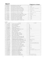
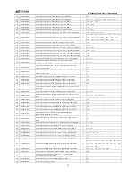
Page 19: ... ADF4111 TSSOP RoHS 1 IC2 10 102 DS2431 001 Memory IC DS2431P TSOC 1 IC17 11 102 FP3502 R01 Regulator IC XC62FP3502PR SOT 89 RoHS 1 IC16 12 102 M2902V R01 Operational Amplifier NJM2902V OP AMP RoHS 1 IC5 13 102 M2904V R01 Operational Amplifier NJM2904V OP AMP RoHS 1 IC3 14 102 W25X40 R01 Memory IC W25X40VSNIG RoHS 1 IC15 15 103 0MA742 R01 Surface Mounted Switch Diode MA742 PANASONIC RoHS 4 D22 D35...

Page 20: ...R60 R109 R113 R114 R115 R116 R120 R127 R234 R237 R261 R270 58 109 040123 R01 Surface Mounted Resistor 0402 12K 5 RoHS 4 R140 R191 R209 R231 59 109 040124 R01 Surface Mounted Resistor 0402 120K 5 RoHS 2 R193 R204 60 109 040151 R01 Surface Mounted Resistor 0402 150R 5 RoHS 1 R100 61 109 040152 R01 Surface Mounted Resistor 0402 1 5K 5 RoHS 3 R13 R28 R180 62 109 040153 R01 Surface Mounted Resistor 040...

Page 21: ...55 R58 R63 R67 R72 106 109 060184 R01 Surface Mounted Resistor 0603 180K 5 RoHS 1 R124 107 109 060220 R01 Surface Mounted Resistor 0603 22R 5 RoHS 1 R27 108 109 060221 R01 Surface Mounted Resistor 0603 220R 5 RoHS 1 R104 109 109 060222 R01 Surface Mounted Resistor 0603 2 2K 5 RoHS 1 R1 110 109 060271 R01 Surface Mounted Resistor 0603 270R 5 RoHS 3 C165 R17 R23 111 109 060273 R01 Surface Mounted Re...

Page 22: ...01 Surface Mounted Capacitor 0402 47P 5 50V C0G RoHS 3 C128 C252 C309 153 112 043471 R01 Surface Mounted Capacitor 0402 470P 10 50V X7R RoHS 86 C6 C7 C21 C23 C31 C34 C43 C46 C49 C56 C57 C58 C62 C63 C65 C67 C71 C73 C76 C77 C78 C79 C80 C81 C82 C85 C86 C92 C94 C97 C98 C100 C109 C110 C113 C119 C125 C126 C127 C131 C133 C 154 112 043473 R01 Surface Mounted Capacitor 0402 0 047uF 10 16V X7R RoHS 1 C238 1...

Page 23: ...1 L23 199 114 06G180 R01 Surface Mounted Inductor MLG1608B18NJT 18nH 5 0603 RoHS 1 L21 200 114 06G181 001 Surface Mounted Multilayer Inductor LGHK1608R18J T 180nH 5 0603 Stop using 1 L7 201 114 06G220 R01 Surface Mounted Inductor MLG1608B22NJT 22nH 5 0603 RoHS 2 L15 L17 202 114 06G221 R02 Surface Mounted Multilayer Inductor LGHK1608R22J T 220nH 5 0603 RoHS 5 L20 L25 L31 L38 L46 203 114 06G270 R01 ...

Page 24: ...ubber PTT Key Silicone Rubber RoHS 1 21 202 006500 R02 PT6500 Main Waterproof Silicone Rubber RoHS 1 22 202 006500 R03 PT6500 Top Waterproof Silicone Rubber RoHS 1 23 202 006500 R05 PT6500 Waterproof for Anode Bracket Silicone Rubber Orange 45 RoHS 1 24 202 006500 R06A PT6500 Numeric Keypad Silicone Rubber Oil Spray Laser Carving RoHS 1 25 203 000558 R07B PT558 Antenna Connector Nickel plated Bras...

Page 25: ... Black Ni plated RoHS 1 49 304 30030G R02 Nonstandard Screw M3 0 3 0 Thick Head Black Ni plated RoHS 1 Appendix 4 Accessories Name Model Specification External View Battery KB 36C 7 4V 1750mAH Li ion Battery Hand Strap KGS 03 KME 68B Earphone KME 68D Charger KBC 60Q 7 hour standard charger Power Adapter KTC 50D1 KA Whip Antenna Antenna KA Stubby Antenna ...

Page 26: ...3 SW ADF4111 MOD Q1 RF POWER APC 5T 450KHZ MUTE TDA8541 SCLK SDATA BUSY1 Q37 SW W588C 5R 12 8MHz X1 TCXO IC13 W588A080 5C TX VCO Q11 RX 5C Q15 4 2ND LOCAL AMP SW CF2 450KHz IC6 AK2346 pin 23 pin 7 MOD pin 7 Q30 HP Q31 HP IC1A HP AMP IC1B IC10 HT9172 IC5A IC5B IC5C IC5D AMP LP LP AMP pin 20 TXD CTCSS DCS DTMF 2T MIC AMP IC14A AMP IC14B Q46 SW MUTE MIC RXD VOX pin 3 5T 5RC Q39 SW 5R SAVE Q44 SW 5C X...

Page 27: ...4 7uF 10V C311 471 C323 471 C336 4 7uF 10V C335 471 Rset 1 CP 2 CPGND 3 AGND 4 RFinB 5 RFinA 6 AVDD 7 REFin 8 DGND 9 CE 10 CLK 11 DATA 12 LE 13 MUXOUT 14 DVDD 15 Vp 16 IC2 ADF4111 R48 4 7K C84 101 R43 560R C96 0 1uF 35V R44 560R R45 2 7K C112 1uF 16V R41 560R C102 0 1uF 35V R46 2 7K C118 1uF 16V L33 BLM11A221S C20 4 7uF 10V C33 104 L9 BLM11A221S C21 471 R2 10R R24 2 7K C61 R47 10R C110 471 C122 4 ...

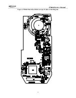
Page 28: ...PT6800 Service Manual 27 Figure 3 PT6800 Main Board Top Layer Position Mark Diagram ...

Page 29: ...PT6800 Service Manual 28 Figure 4 PT6800 Main Board Bottom Layer Position Mark Diagram ...

Page 30: ...PT6800 Service Manual 29 Figure 5 PT6800 Main Board Top Layer Position Value Diagram ...

Page 31: ...PT6800 Service Manual 30 Figure 6 PT6800 Main Board Bottom Layer Position Value Diagram ...

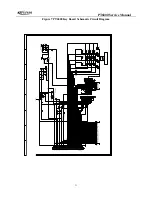
Page 32: ... 2 3 4 5 6 7 8 9 10 CN2 CN10 1 2 3 4 5 6 7 8 9 10 11 12 13 14 15 16 17 18 19 20 21 22 23 24 39 25 26 27 28 29 30 31 32 33 34 35 36 37 38 CN3 CN38 C11 221 C7 221 C6 221 1 2 3 4 5 6 7 8 9 10 11 12 13 14 15 CN1 CN14 L1 BLM11A221S C13 103 C12 102 R4 0R R8 R7 2 7K R6 2 7K R3 2 7K R2 2 7K R1 2 7K L2 BLM11A221S C15 103 C14 102 按键板电原理图 名称 文件号 设计 批准 机型 版本 审核 第 张 张 共 1 1 Q3 2SK1824 R23 R21 100K R5 2 7K C1 2...

Page 33: ...PT6800 Service Manual 32 Figure 8 PT6800 Key Board Top Layer Position Mark Diagram ...

Page 34: ...PT6800 Service Manual 33 Figure 9 PT6800 Key Board Bottom Layer Position Mark Diagram ...

Page 35: ...PT6800 Service Manual 34 Figure 10 PT6800 Key Board Top Layer Position Value Diagram ...

Page 36: ...PT6800 Service Manual 35 Figure 11 PT6800 Key Board Bottom Layer Position Value Diagram ...

Page 37: ...PT6800 Service Manual 36 Figure 12 PT6800 PTT Board Schematic Circuit Diagram 1 1 2 2 3 3 4 4 D D C C B B A A 1 2 3 4 5 6 7 CN1 CN6 SW1 SW2 SW3 R1 20K R2 4 7K PTT 板原理图 名称 文件号 设计 批准 机型 版本 审核 第 张 张 共 1 1 ...

Page 38: ...PT6800 Service Manual 37 Figure 13 PT6800 PTT Board Top Layer Position Mark Diagram Figure 14 PT6800 PTT Board Bottom Layer Position Mark Diagram ...

Page 39: ...PT6800 Service Manual 38 Figure 15 KB 36C Schematic Circuit Diagram L1 1uH L2 1uH L3 0140 05 t TH1 10k C1 1000p Charger T Charger BAT BAT D1 1N5819 2 2k CN1 LTP190 ...

Page 40: ...PT6800 Service Manual 39 Figure 16 KBC 60Q Schematic Circuit Diagram ...

Page 41: ...PT6800 Service Manual 40 Figure 17 PCB Layout 1 ...

Page 42: ...PT6800 Service Manual 41 Figure 18 PCB Layout 2 ...

Reviews: