TR850 Service Manual
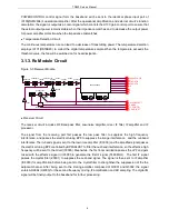
POWERCONTROL control signal form the baseband will be sent to the identical phase input port of
IC100(NJM2904)’s operational amplifier. After the operational amplification and external circuit’s function
calculation, the signal is output as a conrol signal which controls the U100 gain control port to ensure that
the actual output power remains stable when the impedance matches and to decrease the output power
for power amplifier protection when the impedance mismatches.
Temperature Detection Circuit
The continuous temperature rise can lead to a decrease of transmitting power. The temperature detection
employs IC101(DS18B20) to collect the digital temperature sample.When the temperature exceeds the
threshold value, the fan will be switched on for heat dissipation.
3.1.3. Rx Module Circuit
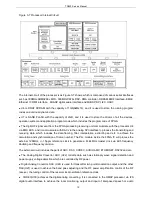
Figure 3-3 Receiver Module
IC6003
FS
DATAOUTB
CLK
DATAOUTA
IC6001
AD9864SY NCB
IC1000
Q1009/1011
U5002
Q2002
PD
PC
PE
PLL
PLL CONFIG
12.8MHz
BPF ADJUST
IC3000
L3006/8/9
L3000/1/2
Z3001
IC3005
L3010/11/12
Z3000
Q3001/2
U4000 AD9864
2rd LO
18MHz CLOCK
IC3003
RXVCOSELECT
Receiver Circuit
The receiver circuit includes RF Band pass filter, Low-noise amplifier, mixer, IF filter, IF amplifier and IF
processor.
The signal from the receiving port first passes the low pass filter to suppress the high frequency
interference, and passes the electrical tuning BPF to suppress the image interference and the out-band
interference.The in-band signal is sent to the low noise amplifier (IC3000) and the amplified signal passes
the electrical tuning BPF controlled by BPFADJUST to filter the out-band interference, so the effective high
frequency will be sent to the mixer(IC3005). Meanwhile, the first local oscillation passes the LPF and gets
mixed with the effective signal in IC3005 to generate the first IF signal (51.65MHz). The first IF signal
passes the crystal filter (Z3001) to suppress the out-band signal. The signal is then sent to IF amplifier
(IC6003) for amplification before being sent to the crystal filter to strenghthen the suppression of the the
adjacent channel. After being sent to the limiting amplifier composed of Q3001 and Q3002, the signal
enters AD9864 (U4000) for the second frequency mixing ,IF amplification and AD sampling. The digital IQ
signal will be finally output to the baseband for further processing.
6
Summary of Contents for TR850
Page 1: ......
Page 45: ...TR850 Service Manual 5 4 Connection 1 2 3 4 6 8 7 5 9 10 13 14 15 16 18 17 11 12 41 ...
Page 90: ...TR850 Service Manual Figure 1 Rx Module Top Board PCB View 86 ...
Page 91: ...TR850 Service Manual Figure 2 Rx Module Bottom Board PCB View 87 ...
Page 93: ...TR850 Service Manual Figure 5 Power Amplifier Module Bottom Board PCB View 89 ...
Page 94: ...TR850 Service Manual Figure 6 Baseband Mainboard Top Board PCB View 90 ...
Page 95: ...TR850 Service Manual Figure 7 Baseband Mainboard Bottom Board PCB View 91 ...
Page 97: ...TR850 Service Manual Figure 10 Power Board Top Board PCB View 93 ...
Page 114: ...TR850 Service Manual Figure 16 Baseband Mainbaord Schematic Diagram 110 ...
Page 169: ...TR850 Service Manual Figure 1 Rx module Top Board Position Mark Diagram 165 ...
Page 170: ...TR850 Service Manual Figure 2 Rx Module Buttom Board Position Mark Diagram 166 ...
Page 172: ...TR850 Service Manual Figure 5 Power Amplifier Module Buttom Position Mark Diagram 168 ...
Page 173: ...TR850 Service Manual Figure 6 Baseband Mainboard Top Board Position Mark Diagram 169 ...
Page 174: ...TR850 Service Manual Figure 7 Baseband Mainboard Buttom Board Position Mark Diagram 170 ...
Page 176: ...TR850 Service Manual Figure 10 Power Board Top Board Position Mark Diagram 172 ...
Page 193: ...TR850 Service Manual Figure 16 Baseband Mainboard Schematic Diagram 189 ...


