TR850 Service Manual
IF Processor Circuit
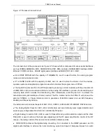
Figure 3-4 IF Processor
The 51.65MHz IF signal output from the IF amplifier enters the AD9864 via its pin 47, and it finishes the
second frequency mixing in the AD9864 to convert the fisrt IF to the second IF. The second IF signal is
converted to the digital signal through the ADC sampling and output from the SSI port, and the digital
signal is sent to FPGA for demodulation.
The reference frequency of AD9864 is 12.8MHz. The second local oscillation VCO is composed of
external oscillation tube, varactor, and related components. The VCO provides the 49.4MHz local
oscillation signal. The clock frequency of AD9864 is18MHz and it is generated by external LC resonance
circuit.
Rx Module Frequency Generation Unit Circuit
The Rx Module Frequency Generation Unit Circuit is composed of two VCOs and one PLL. Two VCOs
cover the band of 400~435MHz and 435~470MHz respectively (VHF is 136~155MHz and 155~174MHz).
a. Working Principle of PLL
The 12.8MHz clock frequency provided by the baseband will enter the frequency divider for division, and
then the 3.2MHz phase detecting frequency will be generated. The signal generated by VCO enters the
PLL chip for frequency division, and goes into the PD to get compared in phase difference with the signal
generated by frequency division of reference clock, thus the continuous pulse current is generated. The
continuous pulse current passes the loop filter and will be converted to CV voltage via RC integral. The CV
voltage will be sent to the varactor, and it controls and adjusts the VCO output frequency until the CV
becomes constant. In the mean time, the PLL is locked, and the stable output frequency from VCO
passes the two buffer amplifier to enter the frequency mixer.
b. Working Principle of VCO
The Rx module employs two VCOs which cover the band of 348.35~383.35MHz and 383.35~418.35MHz
7
Summary of Contents for TR850
Page 1: ......
Page 45: ...TR850 Service Manual 5 4 Connection 1 2 3 4 6 8 7 5 9 10 13 14 15 16 18 17 11 12 41 ...
Page 90: ...TR850 Service Manual Figure 1 Rx Module Top Board PCB View 86 ...
Page 91: ...TR850 Service Manual Figure 2 Rx Module Bottom Board PCB View 87 ...
Page 93: ...TR850 Service Manual Figure 5 Power Amplifier Module Bottom Board PCB View 89 ...
Page 94: ...TR850 Service Manual Figure 6 Baseband Mainboard Top Board PCB View 90 ...
Page 95: ...TR850 Service Manual Figure 7 Baseband Mainboard Bottom Board PCB View 91 ...
Page 97: ...TR850 Service Manual Figure 10 Power Board Top Board PCB View 93 ...
Page 114: ...TR850 Service Manual Figure 16 Baseband Mainbaord Schematic Diagram 110 ...
Page 169: ...TR850 Service Manual Figure 1 Rx module Top Board Position Mark Diagram 165 ...
Page 170: ...TR850 Service Manual Figure 2 Rx Module Buttom Board Position Mark Diagram 166 ...
Page 172: ...TR850 Service Manual Figure 5 Power Amplifier Module Buttom Position Mark Diagram 168 ...
Page 173: ...TR850 Service Manual Figure 6 Baseband Mainboard Top Board Position Mark Diagram 169 ...
Page 174: ...TR850 Service Manual Figure 7 Baseband Mainboard Buttom Board Position Mark Diagram 170 ...
Page 176: ...TR850 Service Manual Figure 10 Power Board Top Board Position Mark Diagram 172 ...
Page 193: ...TR850 Service Manual Figure 16 Baseband Mainboard Schematic Diagram 189 ...


