TR850 Service Manual
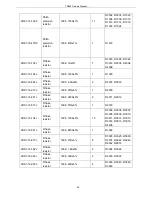
programming cannot be completed, changing NAND FLASH (U7)
for a second modulation and changing the parameter settings is
suggested.
2. Check the DC power supply of the processor unit below:
3V3_OMAP
1V2_OMAP
1V8_DDR
3. Check the DC power supply of the FPGA unit below.
VCCINT(1.2V)
VCCD_PLL(1.2V)
VCCA(2.5V)
VCCIO(3.3V)
4. Check the baseband board 12.8M clock (Y5) and 24M
clock(Y2).
11
Network connection
Fails
1. Check the cable connecting status.
2. Check the internet card chip power.
3. Check the 50M clock of the internet card chip.
12
No voice repeated
Please check Pin2 of transmit unit connector (J17). If there is no
modulation signal, please check reference voltage VREF (2.048V)
of DAC output from U29. If the VREF voltage is abnormal, please
change U29. If VREF is normal, please check DAC (U24).
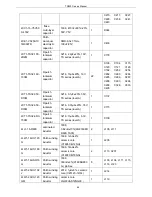
13
No voice outside the
mode.
1.
Check the connecting status of ACCY connecting cable and
connector (U9).
2. Check the 18.432MHz clock of CODEC and power of 3VE_A,
3V3_OMAP. Please input 1KHz and 50mV testing audio signal on
the TXAF test point of baseband board, and check the transmitting
deviation from Comprehensive test instrument. If the deviation is
abnormal, please change CODEC chip (U30).
14
Abnormal
Programming
1. Check the connecting status of network connector (J12) and
network cable.
2. Check the network card running status of PC.
3. Check 50M clock(J23) of network connector on baseband.
4. Check prompt content on the programming running print
information and make the corresponding judgment.
54
Summary of Contents for TR850
Page 1: ......
Page 45: ...TR850 Service Manual 5 4 Connection 1 2 3 4 6 8 7 5 9 10 13 14 15 16 18 17 11 12 41 ...
Page 90: ...TR850 Service Manual Figure 1 Rx Module Top Board PCB View 86 ...
Page 91: ...TR850 Service Manual Figure 2 Rx Module Bottom Board PCB View 87 ...
Page 93: ...TR850 Service Manual Figure 5 Power Amplifier Module Bottom Board PCB View 89 ...
Page 94: ...TR850 Service Manual Figure 6 Baseband Mainboard Top Board PCB View 90 ...
Page 95: ...TR850 Service Manual Figure 7 Baseband Mainboard Bottom Board PCB View 91 ...
Page 97: ...TR850 Service Manual Figure 10 Power Board Top Board PCB View 93 ...
Page 114: ...TR850 Service Manual Figure 16 Baseband Mainbaord Schematic Diagram 110 ...
Page 169: ...TR850 Service Manual Figure 1 Rx module Top Board Position Mark Diagram 165 ...
Page 170: ...TR850 Service Manual Figure 2 Rx Module Buttom Board Position Mark Diagram 166 ...
Page 172: ...TR850 Service Manual Figure 5 Power Amplifier Module Buttom Position Mark Diagram 168 ...
Page 173: ...TR850 Service Manual Figure 6 Baseband Mainboard Top Board Position Mark Diagram 169 ...
Page 174: ...TR850 Service Manual Figure 7 Baseband Mainboard Buttom Board Position Mark Diagram 170 ...
Page 176: ...TR850 Service Manual Figure 10 Power Board Top Board Position Mark Diagram 172 ...
Page 193: ...TR850 Service Manual Figure 16 Baseband Mainboard Schematic Diagram 189 ...


