TR850 Service Manual
3.1.1. Tx Circuit
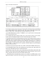
Figure 3-1 Transmitter Circuit
X100
MODE1
SDATA
TXPLLCS
SCLK
TXLD
MODEIN
Q2002
IC100 SKY72310
IC306
U402
TOTXPA
MODE2
TXVCOSELECT
TXVCO2
Q105
Q106
TXENABLE
Transmitter circuit includes three parts:
Two Point Modulation Circuit
The RF center frequency calibration from the baseband and the low frequency part of 4FSK signal will
be processed with addition algorithm, then sent to the DAC to get MODE1 signal. The MODE1 directly
enters the reference clock X100, which is used for center frequency control and low frequency modulation.
The MODE2 signal, which passes the two-level low pass filter which is composed of IC301s for DAC
sampling interference filter, will be sent into VCO for high frequency part modulation.
Transmitter Frequency Generation Unit Circuit
The transmitter PLL includes two VCOs,one PLL(IC100) IC SKY72310 and reference clock X100. The
transmitting frequencies of the two VCOs controlled by the TXVCOSELECT signal are 400~435MHz and
435~470MHz respectively.(VHF is 136~155MHz and 155~174MHz)
a. Working Principle of Voltage Controlled Oscillator
The Tx Module employs two VCOs which cover the band of 400~435MHz and 435~470MHz (VHF is
136~155MHz and 155~174MHz). The switch of VCO is controlled by the TXVCOSELECT signal. VCO
employs three point capacitance oscillation circuit. The VCO that covers the band of 400~435MHz (VHF is
136~155MHz) is composed of D106~D109
、
L119
、
Q106 and some other components, while the VCO
covers the band of 435~470MHz (VHF is 155~174MHz) is composed of D101~D104
、
L107
、
Q105 and
some other components.
b. Working Principle of Frequency Generation Unit
The 12.8 MHz reference clock (X100) output signal which is controlled by MODE1 signal will enter the
reference input port of PLL IC (IC100 SKY72310), then according to the configuration of register, it will be
divided to get 3.2MHz reference frequency, and the frequency will be compared in phase difference with
the signal generated by the frequency division which is resulted from the VCO’s enter into the input port of
PLL chip. The PLL (IC100 SKY72310) PD pin will output the positive or negative pulse current which is in
output pulse width, is directly proportional to the aforementioned signal phase difference. When the pulse
4
Summary of Contents for TR850
Page 1: ......
Page 45: ...TR850 Service Manual 5 4 Connection 1 2 3 4 6 8 7 5 9 10 13 14 15 16 18 17 11 12 41 ...
Page 90: ...TR850 Service Manual Figure 1 Rx Module Top Board PCB View 86 ...
Page 91: ...TR850 Service Manual Figure 2 Rx Module Bottom Board PCB View 87 ...
Page 93: ...TR850 Service Manual Figure 5 Power Amplifier Module Bottom Board PCB View 89 ...
Page 94: ...TR850 Service Manual Figure 6 Baseband Mainboard Top Board PCB View 90 ...
Page 95: ...TR850 Service Manual Figure 7 Baseband Mainboard Bottom Board PCB View 91 ...
Page 97: ...TR850 Service Manual Figure 10 Power Board Top Board PCB View 93 ...
Page 114: ...TR850 Service Manual Figure 16 Baseband Mainbaord Schematic Diagram 110 ...
Page 169: ...TR850 Service Manual Figure 1 Rx module Top Board Position Mark Diagram 165 ...
Page 170: ...TR850 Service Manual Figure 2 Rx Module Buttom Board Position Mark Diagram 166 ...
Page 172: ...TR850 Service Manual Figure 5 Power Amplifier Module Buttom Position Mark Diagram 168 ...
Page 173: ...TR850 Service Manual Figure 6 Baseband Mainboard Top Board Position Mark Diagram 169 ...
Page 174: ...TR850 Service Manual Figure 7 Baseband Mainboard Buttom Board Position Mark Diagram 170 ...
Page 176: ...TR850 Service Manual Figure 10 Power Board Top Board Position Mark Diagram 172 ...
Page 193: ...TR850 Service Manual Figure 16 Baseband Mainboard Schematic Diagram 189 ...


