TR850 Service Manual
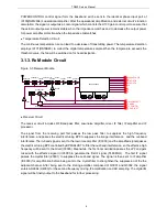
current passes the loop filter, it will be converted to CV voltage via RC integral. The the CV voltage will be
sent to the VCO varactor to adjust and control the output frequency from the VCO until the CV voltage
becomes constant. The loop is locked in the meantime.
Buffer Amplifier Circuit
VCO outputs the modulated carrier signal to enter Q2002 for buffer amplication and then passes the LPF
U402 to eliminate the harmonic wave. After that, the signal will go into IC306 for pre-amplification, then
passes the LPF to filter the harmonic wave again, and the signal is output to the SMA connector which is
connected to the transmitting power amplification.
3.1.2. RF Power Amplifier Module Circuit
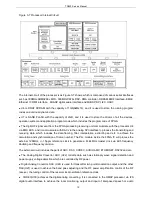
Figure 3-2 RF power amplification module
D103
SWR-R
IC100
POWERCONTROL
IC101
DS18B20
RFOUT
SWR-T
Q102
RF IN
U100
D104
The power amplifier module will amplify the modulated carrier signal from the transmitter module to a
certain power level, then send to the transmitter port.
The power amplifier module includes the three parts:
Power Amplification Part
The modulated carrier from the transmitter module will enter Q102 for pre-amplification, then the signal
will attenuate to a certain level to make the amplitude of the signal which will be input with U100 operates
between 17~20dBm. Under the control of POWERCONTROL signal, the RF signal output from U100 will
pass the LPF to suppress the harmonic wave and collect power stationary wave sample from the
directional coupler before being sent to the antenna port.
APC and Stationary Wave Protection Circuit
The directional coupler detects the forward and reverse directions RF signal and passes the Q103,Q104
to convert the signal to the DC voltage which is corresponding to the forwardand reverse direction power.
After the voltage division, the forward direction DC voltage with the reverse direction voltage pass the
selection switch which is composed of D201,D202 and enter IC100(NJM2904) for buffer amplification
before being sent to the reverse phase input port of the operational amplifier of IC100(NJM2904). The
5
Summary of Contents for TR850
Page 1: ......
Page 45: ...TR850 Service Manual 5 4 Connection 1 2 3 4 6 8 7 5 9 10 13 14 15 16 18 17 11 12 41 ...
Page 90: ...TR850 Service Manual Figure 1 Rx Module Top Board PCB View 86 ...
Page 91: ...TR850 Service Manual Figure 2 Rx Module Bottom Board PCB View 87 ...
Page 93: ...TR850 Service Manual Figure 5 Power Amplifier Module Bottom Board PCB View 89 ...
Page 94: ...TR850 Service Manual Figure 6 Baseband Mainboard Top Board PCB View 90 ...
Page 95: ...TR850 Service Manual Figure 7 Baseband Mainboard Bottom Board PCB View 91 ...
Page 97: ...TR850 Service Manual Figure 10 Power Board Top Board PCB View 93 ...
Page 114: ...TR850 Service Manual Figure 16 Baseband Mainbaord Schematic Diagram 110 ...
Page 169: ...TR850 Service Manual Figure 1 Rx module Top Board Position Mark Diagram 165 ...
Page 170: ...TR850 Service Manual Figure 2 Rx Module Buttom Board Position Mark Diagram 166 ...
Page 172: ...TR850 Service Manual Figure 5 Power Amplifier Module Buttom Position Mark Diagram 168 ...
Page 173: ...TR850 Service Manual Figure 6 Baseband Mainboard Top Board Position Mark Diagram 169 ...
Page 174: ...TR850 Service Manual Figure 7 Baseband Mainboard Buttom Board Position Mark Diagram 170 ...
Page 176: ...TR850 Service Manual Figure 10 Power Board Top Board Position Mark Diagram 172 ...
Page 193: ...TR850 Service Manual Figure 16 Baseband Mainboard Schematic Diagram 189 ...


