Functional Description
AM4011
Page 2 - 10
ID 1022-1626, Rev. 1.0
P R E L I M I N A R Y
2.3.3
General Purpose DIP Switch
The AM4011 is equipped with a general purpose, 4-bit DIP switch, which enables the user to
configure the AM4011 according to his individual needs.
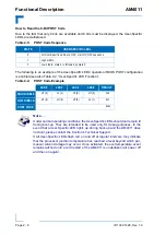
The following table indicates the functions of the four switches integrated in the DIP switch.
For further information on the DIP switch configuration, refer to section 4.1, “DIP Switch Con-
figuration”.
2.3.4
Debug Interface
The AM4011 provides several onboard options for hardware and software debugging, such as:
•
Four bicolor debug LEDs for signaling hardware failures and BIOS POST code
•
An optional ITP700 (processor JTAG) connector J9 is included to facilitate debug and
BIOS software development.
2.3.5
Onboard USB 2.0 NAND Flash Connector
The AM4011 has one onboard USB 2.0 interface for connecting an optional USB 2.0 NAND Flash
mezzanine module. This interface is implemented using the 10-pin connector, J6, with the
following pinout.
Table 2-6:
DIP Switch Functions
SWITCH
FUNCTION
1
POST code display during bootup
2
BIOS Firmware Hub configuration
3
Set the default boot order configuration
4
Clearing BIOS CMOS parameters
Figure 2-3: USB NAND Flash Con. J6
1
9
2
10
Table 2-7: USB NAND Flash Con. J6 Pinout
PIN
SIGNAL
FUNCTION
I/O
1
VCC
VCC
--
3
UV0-
Differential USB-
I/O
5
UV0+
Differential USB+
I/O
7
GND
GND
--
9
Key
2, 4, 6, 8 NC
Not connected
--
10
Res.
Reserved
--


