Functional Description
AM4011
Page 2 - 22
ID 1022-1626, Rev. 1.0
P R E L I M I N A R Y
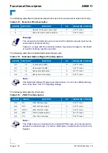
The following table lists the reserved pins which must not be connected to external circuitry.
The following table lists the Extended Options Region pins:
The following table lists the JTAG pins:
Table 2-13: Reserved Pins Description
AMC PIN
AMC PORT
FUNCTION
I/O
SIGNALING VOLTAGE
6
--
Optional PCI Express reset output
O
3.3V TTL level
8
--
Reserved input for general purpose
I
3.3V TTL level
Warning!
The reserved pins listed above are reserved for optional use and must not be
connected to external circuitry.
Failure to comply with the instruction above may cause damage to the board
or result in improper system operation.
Table 2-14: Extended Options Region Pins Description
AMC PIN
AMC PORT
FUNCTION
I/O
SIGNALING VOLTAGE
133
15
Tx serial port (COM2)
O
3.3V TTL level
132
15
Rx serial port (COM2)
I
3.3V TTL level
127
14
Debug serial data output
O
3.3V TTL level
126
14
Debug serial clock output
O
3.3V TTL level
Note ...
The Extended Options Region pins listed above do not have differential sig-
nals. They have 3.3V TTL signaling voltage.
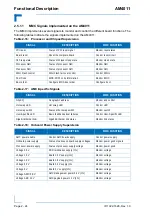
Table 2-15: JTAG Pins Description
AMC PIN
SIGNAL
FUNCTION
I/O
SIGNALING VOLTAGE
169
TDI
JTAG Test Data Input
I
3.3V TTL level
168
TDO
JTAG Test Data Output
O
3.3V TTL level
167
TRST#
JTAG Test Reset Input
I
3.3V TTL level
166
TMS
JTAG Test Mode Select In
I
3.3V TTL level
165
TCK
JTAG Test Clock Input
I
3.3V TTL level
Note ...
The JTAG pins are connected to the onboard FPGA logic and can be used to
update the onboard logic. For further information, contact Kontron’s Technical
Support.


