background image

COMe-bSL6 – User Guide Rev. 1.4 


www.kontron.com 

// 38 


2.8.


MTBF  

The following MTBF (Mean Time Before Failure) values were calculated using a combination of manufacturer’s test 
data, if the data was available, and the Telcordia (Bellcore) issue 2 calculation for the remaining parts. 

The Telcordia calculation used is “Method 1 Case 3” in a ground benign, controlled environment (GB,GC). This 
particular method takes into account varying temperature and stress data and the system is assumed to have not 
been burned in. 

Figure 2 below shows MTBF de-rating for the E1 temperature range in an office or telecommunications environment. 
Other environmental stresses (such as extreme altitude, vibration, salt-water exposure) lower MTBF values. 

System MTBF (hours) = 467598 @ 40°C (Reliability report article number 36030-0000-28-8) 


Table 22: MTBF Temperature de-Rating


The above estimates assume no fan, but a passive heat sinking arrangement. Estimated RTC 
battery life (as opposed to battery failures) is not accounted for in the above figure and 
needs to be considered separately. Battery life depends on both temperature and operating 
conditions. When the Kontron unit has external power, the only battery drain is from leakage 
paths. 


Summary of Contents for COMe-bSL6

Page 1: ... USER GUIDE COMe bSL6 Doc User Guide Rev 1 4 Doc ID 1060 7484 ...

Page 2: ...COMe bSL6 User Guide Rev 1 4 www kontron com 2 This page has been intentionally left blank ...

Page 3: ...itable for the specified use without further testing or modification Kontron expressly informs the user that this user guide only contains a general description of processes and instructions which may not be applicable in every individual case In cases of doubt please contact Kontron This user guide is protected by copyright All rights are reserved by Kontron No part of this document may be reprod...

Page 4: ...ns is entirely at your risk To minimize the risks associated with your products and applications you should provide adequate design and operating safeguards You are solely responsible for compliance with all legal regulatory safety and security related requirements concerning your products You are responsible to ensure that your systems and any Kontron hardware or software components incorporated ...

Page 5: ...se Order Terms Conditions Visit http www kontron com terms and conditions For contact information refer to the corporate offices contact information on the last page of this user guide or visit our website CONTACT US Customer Support Find Kontron contacts by visiting http www kontron com support Customer Service As a trusted technology innovator and global solutions provider Kontron extends its em...

Page 6: ...ted and or prescribed by the law may endanger your life health and or result in damage to your material ESD Sensitive Device This symbol and title inform that the electronic boards and their components are sensitive to static electricity Care must therefore be taken during all handling operations and inspections of this product in order to ensure product integrity at all times HOT Surface Do NOT t...

Page 7: ...erforming any work on this product Earth ground connection to vehicle s chassis or a central grounding point shall remain connected The earth ground cable shall be the last cable to be disconnected or the first cable to be connected when performing installation or removal procedures on this product Special Handling and Unpacking Instruction ESD Sensitive Device Electronic boards and their componen...

Page 8: ...roduct then re pack it in the same manner as it was delivered Special care is necessary when handling or unpacking the product See Special Handling and Unpacking Instruction Quality and Environmental Management Kontron aims to deliver reliable high end products designed and built for quality and aims to complying with environmental laws regulations and other environmentally oriented requirements F...

Page 9: ...or 20 2 3 3 Chipset 23 2 3 4 System Memory 23 2 3 5 Graphics 24 2 3 6 LVDS 24 2 3 7 Audio 25 2 3 8 PCI Express PCIE Configuration 25 2 3 9 USB 27 2 3 10 SATA 27 2 3 11 Ethernet 28 2 3 12 COMe High Speed Interfaces 29 2 3 13 Storage Features 29 2 3 14 BIOS Software Features 29 2 3 15 COMe Features 30 2 3 16 Kontron Features 30 2 4 Electrical Specification 31 2 4 1 Power Supply Voltage 31 2 4 2 Powe...

Page 10: ... Security Solution 44 3 11 SpeedStep Technology 44 4 System Resources 46 4 1 Interrupt Request IRQ Lines 46 4 2 Memory Area 46 4 3 I O Address Map 47 4 4 Peripheral Component Interconnect PCI Devices 49 4 5 I2C Bus 49 4 6 System Management SM Bus 49 5 Interface Connectors X1A and X1B 50 5 1 X1A and X1B Signals 50 5 2 X1A and X1B Pin Assignment 51 5 2 1 Connector X1A Row A 52 5 2 2 Connector X1A Ro...

Page 11: ... Fan Connector 35 Table 19 Temperature Grade Specifications 36 Table 20 Humidity Specifications 36 Table 21 Standards and Certifications 37 Table 22 MTBF Temperature de Rating 38 Table 23 Supported BIOS Features 40 Table 24 SPI Boot Pin Configuration 40 Table 25 Supported SPI Boot Flash Types for 8 SOIC Package 41 Table 26 Reserved SM Bus Addresses for Smart Battery Solutions on the Carrier 42 Tab...

Page 12: ...nu Initial Screen 67 Figure 6 System Agent Configuration Menu Initial Screen 78 Figure 7 PCH IO Configuration Menu Initial Screen 82 Figure 8 Security Setup Menu Initial Screen 88 Figure 9 Boot Setup Menu Initial Screen 89 Figure 10 Save and Exit Setup Menu Initial Screen 90 ...

Page 13: ...ncludes 8x PCIe x1 1x PEG x16 1x 1 GbE Support for the Industrial temperature environment 1 2 Product Naming Clarification COM Express defines a Computer On Module or COM with all the components necessary for a bootable host computer packaged as a super component The product names for Kontron COM Express Computer on Modules consist of Short form of the industry standard COMe Module form factor b b...

Page 14: ...ct highly integrated computers All Kontron COM Express modules feature a standardized form factor and a standardized connector layout that carry a specified set of signals Each COM is based on the COM Express specification This standardization allows designers to create a single system baseboard that can accept present and future COM Express modules The baseboard designer can optimize exactly how ...

Page 15: ... 8 GHz CM236 GT4e 45 W 35 W vPro non ECC ECC 38030 0000 20 7 COMe bSL6 i7 6822EQ QM170 Core i7 6822EQ 4x 2 0 GHz QM170 GT2 25 W vPro non ECC 38030 0000 28 7 COMe bSL6 i7 6820EQ QM170 Core i7 6820EQ 4x 2 8 GHz QM170 GT2 45W vPro non ECC 38030 0000 19 5 COMe bSL6 i5 6442EQ QM170 Core i5 6442EQ 4x1 9 GHz QM170 GT2 25W vPro non ECC 36030 0000 27 5 COMe bSL6 i5 6440EQ QM170 Core i5 6440EQ 4x2 7 GHz QM1...

Page 16: ... Support Table 3 R E2S Modules R E2S 40 C to 85 C Product Number Product Name Comment 38031 0000 16 2 COMe bSL6R E2S G3902E CM236 Celeron 3902E 2x 1 6 GHz CM236 GT1 25 W non ECC ECC 38031 0000 24 2 COMe bSL6R E2S G3900E CM236 Celeron 3900E 2x 2 4 GHz CM236 GT1 35 W non ECC ECC 38031 0000 19 3 COMe bSL6R E2S i3 6102E CM236 Core i3 6102E 2x 1 9 GHz CM236 GT2 25 W non ECC ECC 38031 0000 27 3 COMe bSL...

Page 17: ... 7 ADA Type6 DP3 DVO6 sandwich Adapter Card for 3x DisplayPort 96006 0000 00 2 COMe POST T6 NFCB POST Code Debug Card 38019 0000 00 0 ADA COMe Height dual EERC Height Adapter Part Number COMe Starter kit Project Code Comment 38114 0000 00 S COMe Ref Starter kit T6 ADAS Starter kit with COMe Reference Carrier T6 38106 0000 00 S COMe Eval Starter kit T6 Topanga Canyon Starter kit with COMe Evaluatio...

Page 18: ...1200MHz PC4 2400 SODIMM 97017 4096 24 2 DDR4 2400 SODIMM 4 GB E2_COM DDR4 2400 4GB E2 260P 1200MHz PC4 2400 SODIMM 97017 8192 24 2 DDR4 2400 SODIMM 8 GB E2_COM DDR4 2400 8GB E2 260P 1200MHz PC4 2400 SODIMM 97017 1600 24 2 DDR4 2400 SODIMM 16 GB E2_COM DDR4 2400 16GB E2 260P 1200MHz PC4 2400 SODIMM Part Number Memory ECC validated reference types 97018 4096 24 0 DDR4 2400 SODIMM 4 GB ECC_COM DDR4 2...

Page 19: ... Guide Rev 1 4 www kontron com 19 2 3 Functional Specification 2 3 1 Block Diagram COMe bSL6 The following figure displays the system block diagram applicable to all COMe bSL6 modules Figure 1 Block Diagram COMe bSL6 ...

Page 20: ...Technology excluding i5 6662EQ i5 6440EQ G3902E and G3900E Intel TSX NI excluding G3902E and G3900E Idle States Enhanced Intel Speedstep Technology Thermal Monitoring Technologies Intel Flex Memory Access E3 1515M and E3 1505M only Intel Identity Protection Technology excluding E3 1505L Intel Stable Image Platform Program SIPP E3 1515M and E3 1505M only Intel Smart Response Technology E3 1515M and...

Page 21: ...Turbo Frequency 3 7 GHz 3 7 GHz 2 8 GHz 2 8 GHz 3 5 GHz 2 7 GHz Thermal Design Power TDP 45 W 45 W 25 W 25 W 45 W 25 W TDP down 35 W 35 W Smartcache 8 MB 8 MB 8 MB 8 MB 8 MB 6 MB Memory Types DDR4 2133 LPDDR3 1866 DDR3L 1600 DDR4 2133 LPDDR3 1866 DDR3L 1600 DDR4 2133 LPDDR3 1866 DDR3L 1600 DDR4 2133 LPDDR3 1866 DDR3L 1600 DDR4 2133 LPDDR3 1866 DDR3L 1600 DDR4 2133 LPDDR3 1866 DDR3L 1600 Max Memory...

Page 22: ...GHz 2 4 GHz Max Turbo Frequency 3 4 GHz 2 7 GHz Thermal Design Power TDP 45 W 35 W 25 W 25 W 35 W TDP down Smartcache 6 MB 3 MB 3 MB 2 MB 2 MB Memory Types DDR4 2133 LPDDR3 1866 DDR3L 1600 DDR4 2133 LPDDR3 1866 DDR3L 1600 DDR4 2133 LPDDR3 1866 DDR3L 1600 DDR4 1866 2133 DDR3L 1333 1600 1 35V DDR4 1866 2133 DDR3L 1333 1600 1 35V Max Memory Channels 2 2 2 2 2 Max Memory Size 64 GB 64 GB 64 GB 64 GB 6...

Page 23: ...n be determined through the memory module s SPD register The table below lists the operating memory frequencies based on the combination of DIMMs and processors DIMM Type Module Name Memory Data Transfers MT s Processor System Bus Frequency MHz Resulting Memory Clock Frequency MHz Peak Transfer Rate MB s DDR4 2133 PC4 17000 2133 33 2133 266 76 17066 67 For a list of Kontron memory modules see Tabl...

Page 24: ... 60 Hz 24 bpp DP 4096 x 2304 60 Hz 24 bpp HDMI 1 4 native 4096 x 2160 24 Hz 24 bpp HDMI 2 0 via LS Pcon 4096 x 2160 60 Hz 24 bpp VGA 1920 x 1200 60 Hz 24 bpp The maximum resolution is based on the implementation of four lanes with HBR2 link data rates and assumes maximum VCC If more than one active display port is connected then the processor frequency may be lower than base frequency in thermally...

Page 25: ...Storage Device 1 PCIE1 16 PCIe 10 PCIE2 17 PCIe 11 PCIE3 18 PCIe 12 PCIE4 7 PCIe 1 PCIE5 8 PCIe 2 PCIE6 9 PCIe 3 PCIE7 10 PCIe 4 2 3 8 2 PCI Express Graphics x16 PEG Port The PCI Express Graphics x 16 PEG port is available on the COMe connector The configuration is changeable with 1x 16 as default If more than one device is connected then the device with the highest lane count should be connected ...

Page 26: ...11 11 3 3 Lane 12 12 4 0 Linked with 0 1 2 Segment Bus Device Lane 13 13 5 1 Lane 14 14 6 2 Lane 15 15 7 3 Table 11 PCI Express Graphics x16 PEG Port Bifurcation and Lane Reversal Mapping COMe PEG 1x16 Reversed 2x8 Reversed 1x8 2x4 Reversed Lane 0 15 Linked with 0 1 0 Segment Bus Device 7 Linked with 0 1 1 Segment Bus Device 3 Linked with 0 1 2 Segment Bus Device Lane 1 14 6 2 Lane 2 13 5 1 Lane 3...

Page 27: ... 3 0 Comments 0 USB2_1 USB3_1 USB 3 USB 2 0 1 USB2_2 USB3_2 2 USB2_3 USB3_3 3 USB2_4 USB3_4 4 USB2_5 USB 2 0 5 USB2_6 6 USB2_7 7 USB2_8 The PCH implements an xHCI USB controller that provides support for up to 14 USB 2 0 signals pairs 10 SuperSpeed USB 3 0 signal pairs with support for up to 64 devices and 128 endpoints The xHCI controller supports wake up from sleep states S1 S4 2 3 10 SATA The S...

Page 28: ...IPv4 and IPv6 Receive Side Scaling RSS Dual Tx and Rx queues Jumbo Frame Support for up to 9 KB Teaming Shared Flash with system BIOS Server Operating System support Network proxy ARP support 32 Wake Filter support If the LAN Cable is disconnected the ULP Ultra Low Power driver featured under Windows 8 1 and Windows 10 can cause undefined LED behavior To disable ULP use the Intel ULPenable Utility...

Page 29: ...CIE6 9 PCIe 3 PCI express lane 0 15 PCIE5 8 PCIe 2 PCI express lane 0 15 PCIE4 7 PCIe 1 PCI express lane 0 15 USB_SS3 4 USB3_4 USB 3 0 USB_SS2 3 USB3_3 USB 3 0 USB_SS1 2 USB3_2 USB 3 0 USB_SS0 1 USB3_1 USB 3 0 2 3 13 Storage Features The following table lists the on board storage features Serial ATA 4x SATA 6GB s SATA AHCI NCQ HotPlug Staggered Spinup eSATA PortMultiplier 2 3 14 BIOS Software Feat...

Page 30: ...m an external SPI LPC Supported UART 2x UART RX TX LID Signals Supported Sleep Signals Supported SMBus Supported Audio HD Audio for external HAD codecs 2 3 16 Kontron Features The following table lists specific Kontron features External I2C Bus Fast I2C MultiMaster capable M A R S Support Supported Embedded API KEAPI3 Custom BIOS Settings Flash Backup Supported Watchdog Support Triple Staged ...

Page 31: ...minal VCC To comply with the ATX specification there must be a smooth and continuous ramp of each DC input voltage from 10 to 90 of the DC input voltage final set point 2 4 3 Power Supply Voltage Ripple The maximum power supply voltage ripple is 100 mV peak to peak at 0 MHz to 20 MHz 2 4 4 Power Consumption The maximum power consumption of the different COMe bSL6 variants is 36 W to 60 W The follo...

Page 32: ...r seconds turns off power to the module Power Button Override Power Good PWR_OK Pin B24 PWR_OK is internally pulled up to 3 3 V and must be at the high level to power on the module This can be driven low to hold the module from powering up as long as needed The carrier needs to release the signal when ready Low level prevents the COM3 module from entering the S0 state A falling edge during S0 will...

Page 33: ...5 high low 5V high 0V S5 S0 PWRBTN Event low high 5V high low 0 V VCC S0 high high 5V low VCC x Defines that there is no difference if connected or open 2 4 7 2 Single Supply Mode In single supply mode without 5V standby the module starts automatically when VCC power is connected and Power Good input is open or at high level internal PU to 3 3 V PS_ON is not used in this mode and VCC can be 8 5 V ...

Page 34: ...s provided from Kontron for the COMe bSL6 are usually designed to cover the power and thermal dissipation for a commercial temperature range used in housing with proper airflow 2 5 2 Operating with Kontron Heatspreader Plate HSP Assembly The operating temperature defines two requirements Maximum ambient temperature with ambient being the air surrounding the module Maximum measurable temperature on...

Page 35: ...f the following adaptor cables KAB HSP 200 mm PN 96079 0000 00 0 KAB HSP 40 mm PN 96079 0000 00 2 If the input voltage is below 13 V the maximum supply current to the on module fan connector is 350 mA The maximum supply current is limited to 150 mA if the input voltage is between 13 V and 20 V Always check the fan specification according to the limitations of the output current Table 18 Electrical...

Page 36: ... Chapter 2 1 Module Variants Table 19 Temperature Grade Specifications Temperature Grades Operating Storage Non operating Validated Input Voltage Commercial Grade 0 C to 60 C 40 C to 85 C VCC 8 5 V 20 V Extended Temperature E1 25 C to 75 C 30 C to 85 C VCC 12 V Industrial Grade by Screening E2S 40 C to 85 C or custom 40 C to 85 C VCC 12 V 2 6 2 Humidity Table 20 Humidity Specifications Humidity 93...

Page 37: ... EN 61000 4 3 Radiated field immunity IEC EN 61000 4 4 Electrical fast transient burst EFT burst IEC EN 61000 4 5 Surge immunity test IEC EN 61000 4 6 Immunity to conducted disturbances IEC EN 61000 4 8 Power frequency magnetic field Immunity IEC EN 61000 4 11 Voltage dips short interruptions voltage variation immunity Safety EN 62368 1 2014 Safety for audio video and information technology equipm...

Page 38: ... in Figure 2 below shows MTBF de rating for the E1 temperature range in an office or telecommunications environment Other environmental stresses such as extreme altitude vibration salt water exposure lower MTBF values System MTBF hours 467598 40 C Reliability report article number 36030 0000 28 8 Table 22 MTBF Temperature de Rating The above estimates assume no fan but a passive heat sinking arran...

Page 39: ...ion defines a module height of approximately 13 mm from module PCB bottom to heatspreader top as shown in the figure below Figure 3 Module Height Cooling solutions provided by Kontron for basic sized Computer on Modules are 27 mm in height from module bottom to heatsink top Universal Cooling solutions to be mounted on the heatspreader are 14 3 mm in height for an overall height of 27 3 mm from mod...

Page 40: ...Supported BIOS Features 3 3V 83627DHG P AMI EFI APTIO V PS 2 Not specified COM1 COM2 Supported LPT Supported HWM Not supported Floppy Not supported GPIO Not supported Features marked as not supported do not exclude OS support e g HWM is accessible via SMB If any other LPC Super I O additional BIOS implementations are necessary contact Kontron Support 3 2 Serial Peripheral Interface SPI The Serial ...

Page 41: ...0 and pin B88 BIOS_DIS1 to boot from the module BIOS 3 Turn on the system and make sure your USB is connected then start the setup See Chapter6 1 Starting the uEFI BIOS 4 Check that the following entries are set to their default setting Advanced PCH FW Configuration Firmware update configuration ME FW Image Re Flash Disabled Advanced PCH FW Configuration Firmware update configuration Local FW Upda...

Page 42: ...er M A R S includes support for a SMBus charger selector e g Linear Technology LTC1760 Dual Smart Battery System Manager and provides ACPI compatibility to report battery information to the operating system Table 26 Reserved SM Bus Addresses for Smart Battery Solutions on the Carrier 8 bit Address 7 bit Address Device 12h 0x09 SMART_CHARGER 14h 0x0A SMART_SELECTOR 16h 0x0B SMART_BATTERY 3 4 Fast I...

Page 43: ... by standard interrupt masking techniques in the system It is used typically to signal attention for non recoverable hardware errors 0011b SMI A system management interrupt SMI makes the processor entering the system management mode SMM As such specific BIOS code handles the interrupt The current BIOS handler for the watchdog SMI currently does nothing For special requirements contact Kontron Supp...

Page 44: ...CPU Each TPM chip contains an RSA key pair called the Endorsement Key EK The pair is maintained inside the chip and cannot be accessed by software The Storage Root Key SRK is created when a user or administrator takes ownership of the system This key pair is generated by the TPM based on the Endorsement Key and an owner specified password A second key called an Attestation Identity Key AIK protect...

Page 45: ...o the high frequency allowing you to customize performance In order to use the Intel Enhanced SpeedStep technology the operating system must support SpeedStep technology By deactivating the SpeedStep feature in the BIOS manual control or modification of the CPU performance is possible Setup the CPU Performance State in the BIOS Setup or use third party software to control the CPU Performance State...

Page 46: ...vices 12 PS 2 mouse Free for PCI devices 13 FPU FPU 14 IDE0 Not used 15 IDE1 Not used 4 2 Memory Area The following table specifies the memory address range and COMe bSL6 memory usage Designated memory Locations Address Range hex Size Project Usage 00000000 0009FBFF 639 KB Real mode memory 0009FC00 0009FFFF 1 KB Extended BDA 000A0000 000BFFFF 128 KB Display memory legacy 000C0000 000CBFFF 48 KB VG...

Page 47: ...020 021 024 025 028 029 02C 02D 030 031 034 035 038 039 03C 03D Interrupt Controller Master 8259 Interrupt Controller Master 8259 02E 02F SuperIO Winbond External SuperIO Winbond 040 043 050 053 Programmable Interrupt Timer 8253 Programmable Interrupt Timer 8253 04E 04F 2nd SuperIO TPM etc TPM 060 064 KBD Interface Controller 8042 KBD Interface Controller 8042 061 063 065 067 NMI Controller NMI Co...

Page 48: ...used 378 37F Parallel port LPT 1 LPT1 If SuperIO present 3BC 3BF Parallel port LPT3 Not used 3C0 3CF VGA EGA VGA EGA 3D0 3DF CGA Not used 3E0 3E1 PCMCIA ExCA interface Not used 3E8 3EF Serial port COM3 Serial port COM3 optional 3F0 3F7 Floppy Disk Controller Not used 3F6 3F7 HDD controller IDE0 Slave Not used 3F8 3FF Serial Port COM1 Serial port COM1 4D0 4D1 Interrupt Controller Slave Interrupt Co...

Page 49: ...OM No Module EEPROM AEh FRU EEPROM No Recommended for Baseboard EEPROM 4 6 System Management SM Bus The 8 bit SMBus address uses the LSB Bit 0 for the direction of the device Bit0 0 defines the write address Bit0 1 defines the read address The 8 bit address listed below shows the write address for all devices The7 bit SMBus address shows the device address without bit0 Designated I O Port Addresse...

Page 50: ... connectors X1A and X1B Figure 4 X1A and X1B COMe Interface Connectors 5 1 X1A and X1B Signals For a description of the terms used in the X1A and X1B pin assignment tables see Table 28 General Signals Description table or Appendix A List of Acronyms If a more detailed pin assignment description is required refer to the PICMG specification COMe Rev 2 1 Type 6 standard The information provided under...

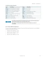
Page 51: ...5 V Tolerance PU Pull Up Resistor OA Output Analog PWR Power Connection OD Output Open Drain and Differential Pair Differentiator To protect external power lines of peripheral devices make sure that the wires have the right diameter to withstand the maximum available current The enclosure of the peripheral device fulfills the fire protection requirements of IEC EN60950 5 2 X1A and X1B Pin Assignme...

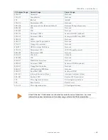
Page 52: ... ATX supply O 3 3 PD 10 kΩ A16 SATA0_TX SATA transmit data pair 0 DP O A17 SATA0_TX A18 SUS_S4 Indicates system is in Suspend to Disk or deeper state O 3 3 PD 10 kΩ A19 SATA0_RX SATA receive data pair 0 DP I A20 SATA0_RX A21 GND Power Ground PWR GND A22 SATA2_TX SATA transmit data pair 2 DP O A23 SATA2_TX A24 SUS_S5 Indicates system is in Soft Off state O 3 3 A25 SATA2_RX SATA receive data pair 2 ...

Page 53: ...t 0 I 3 3 PU 10 kΩ 3 3 V S0 A50 LPC_SERIRQ Serial interrupt request I OD 3 3 PU 8 2 kΩ 3 3 V S0 A51 GND Power Ground PWR GND A52 PCIE_TX5 PCI Express transmit lane 5 DP O A53 PCIE_TX5 A54 GPI0 General purpose input 0 I 3 3 PU 100 kΩ 3 3 V S0 A55 PCIE_TX4 PCI Express transmit lane 4 DP O A56 PCIE_TX4 A57 GND Power Ground PWR GND A58 PCIE_TX3 PCI Express transmit lane 3 DP O A59 PCIE_TX3 A60 GND Pow...

Page 54: ...erted A93 GPO0 General Purpose Output 0 O 3 3 PD 100kΩ A94 SPI_CLK SPI clock Clock from Module to Carrier SPI O 3 3 PU 15 kΩ to 40 kΩ in PCH S5 All SPI signals tri stated with 20 KΩ CPU internal weak pull up until reset deasserted A95 SPI_MOSI SPI Master Out Slave In Data out from Module to Carrier SPI O 3 3 A96 TPM_PP TPM Physical Presence I 3 3 PD 10kΩ TMP does not use this functionality A97 TYP...

Page 55: ...an be used to generate a SMI or to wake the system I O 3 3 PU 2 2 kΩ 3 3 V S5 B16 SATA1_TX SATA 1 transmit data pair DP O B17 SATA1_TX B18 SUS_STAT Indicates imminent suspend operation used to notify LPC devices O 3 3 B19 SATA1_RX SATA 1 receive data pair DP I B20 SATA1_RX B21 GND Power Ground PWR GND B22 SATA3_TX SATA 3 transmit data pair DP O B23 SATA3_TX B24 PWR_OK Power OK from main power supp...

Page 56: ... Express receive lane 5 DP I B53 PCIE_RX5 B54 GPO1 General Purpose Output 1 O 3 3 PD 100 kΩ B55 PCIE_RX4 PCI Express receive lane 4 DP I B56 PCIE_RX4 B57 GPO2 General Purpose Output 2 O 3 3 PD 100 kΩ B58 PCIE_RX3 PCI Express receive lane 3 DP I B59 PCIE_RX3 B60 GND Power Ground PWR B61 PCIE_RX2 PCI Express receive lane 2 DP I B62 PCIE_RX2 B63 GPO3 General Purpose Output 3 O 3 3 PD 100 kΩ B64 PCIE_...

Page 57: ...itor O 3 3 B95 VGA_DDC_CLK Display Data Channel DDC clock line I O 5 PU 2 4 kΩ 3 3 V S0 B96 VGA_DCC_DATA Display Data Channel DDC data line I O 5 PU 2 4 kΩ 3 3 V S0 B97 SPI_CS Chip select for carrier board SPI 0 3 3 B98 RSVD Reserved for future use NC B99 RSVD B100 GND Power Ground PWR GND B101 FAN_PWMOUT Fan speed control by PWM Output O 3 3 20 V protection circuit implemented on module PD on car...

Page 58: ...B_SSRX3 C14 GND Power Ground PWR GND C15 DDI1_PAIR6 NC NC C16 DDI1_PAIR6 C17 RSVD Reserved for future use NC C18 RSVD C19 PCIE_RX6 PCI Express receive lane pair 6 DP I C20 PCIE_RX6 C21 GND Power Ground PWR GND C22 PCIE_RX7 PCI Express receive lane pair 7 DP I C23 PCIE_RX7 C24 DDI1_HPD DDI Hotplug Detect I 3 3 PD 100 kΩ C25 DDI1_PAIR4 NC NC C26 DDI1_PAIR4 C27 RSVD Reserved for future use NC C28 RSV...

Page 59: ...EG_RX3 PCI Express Graphics PEG receive lane 3 DP I C62 PEG_RX3 C63 RSVD Reserved for future use NC C64 RSVD C65 PEG_RX4 PCI Express Graphics PEG receive lane 4 DP I C66 PEG_RX4 C67 RSDN Rapid Shutdown Trigger Input I 5 Used for rapid shutdown option C68 PEG_RX5 PCI Express Graphics PEG receive lane 5 DP I C69 PEG_RX5 C70 GND Power Ground PWR GND C71 PEG_RX6 PCI Express Graphics PEG receive lane 6...

Page 60: ...G_RX13 C96 GND Power Ground PWR GND C97 RSVD Reserved for future use NC C98 PEG_RX14 PCI Express Graphics PEG receive lane 14 DP I C99 PEG_RX14 C100 GND Power Ground PWR GND C101 PEG_RX15 PCI Express Graphics PEG receive lane 15 DP I C102 PEG_RX15 C103 GND Power Ground PWR GND C104 VCC_12V Main input voltage 4 75 V 20 V PWR 4 75 V 20 V C105 VCC_12V C106 VCC_12V C107 VCC_12V C108 VCC_12V C109 VCC_1...

Page 61: ... D15 DDI1_CTRLCLK_AUX DDI1 Clock I O 3 3 PD 100 kΩ D16 DDI1_CTRLDATA_AUX DDI1 Date I O 3 3 PU 100 kΩ 3 3 V S0 D17 RSVD Reserved for future use NC D18 RSVD D19 PCIE_TX6 PCI Express transmit lane pair 6 DP O D20 PCIE_TX6 D21 GND Power Ground PWR GND D22 PCIE_TX7 PCI Express transmit lane pair 7 DP O D23 PCIE_TX7 D24 RSVD Reserved for future use NC D25 RSVD D26 DDI1_PAIR0 DDI1 pair 0 DP O D27 DDI1_PA...

Page 62: ... D67 GND Power Ground PWR GND D68 PEG_TX5 PCI Express Graphics PEG transmit lane 5 DP O D69 PEG_TX5 D70 GND Power Ground PWR GND D71 PEG_TX6 PCI Express Graphics PEG transmit lane 6 DP O D72 PEG_TX6 D73 GND Power Ground PWR GND D74 PEG_TX7 PCI Express Graphics PEG transmit lane 7 DP O D75 PEG_TX7 D76 GND Power Ground PWR GND D77 RSVD Reserved for future use NC D78 PEG_TX8 PCI Express Graphics PEG ...

Page 63: ...ics PEG transmit lane 14 DP O D99 PEG_TX14 D100 GND Power Ground PWR GND D101 PEG_TX15 PCI Express Graphics PEG transmit lane 15 DP O D102 PEG_TX15 D103 GND Power Ground PWR GND D104 VCC_12V Main input voltage 4 75 V 20 V PWR 4 75 V 20V D105 VCC_12V D106 VCC_12V D107 VCC_12V D108 VCC_12V D109 VCC_12V D110 GND Power Ground PWR GND and Differential pair differentiator ...

Page 64: ...low 1 Power on the board 2 Wait until the first characters appear on the screen POST messages or splash screen 3 Press the DEL key 4 If the uEFI BIOS is password protected a request for password will appear Enter either the User Password or the Supervisor Password see Chapter 6 2 4 Security Setup Menu press RETURN and proceed with step 5 5 A Setup menu appears The COMe bSL6 uEFI BIOS Setup program...

Page 65: ...p menus The currently active menu and the currently active uEFI BIOS Setup item are highlighted in white Each Setup menu provides two main frames The left frame displays all available functions Configurable functions are displayed in blue Functions displayed in grey provide information about the status or the operational configuration The right frame displays an Item Specific Help window providing...

Page 66: ...PCH information Name PCH SKU Stepping and Hsio Revision Displays SPI Clock Information Read ID Status Clock Frequency Write and Erase Clock Frequency and Fast Read Clock Frequency Read Clock Frequency Displays Firmware Information ME FWVersion and ME Firmware SKU System Language Selects system default language English Platform Information Read only field Displays Module Information Product Name Re...

Page 67: ...up menu Sub screens and Functions Sub Screen Function Second level Sub Screen Description CPU Configuration Read only field Displays CPU Information Type ID Speed L1 Data Cache L1 Instruction Cache L2 Cache L3 Cache L4 Cache VMX and SMX TXT Intel VMX Virtualization Technology Enables VMM to utilize additional hardware capabilities provided by Vanderpool Technology Enabled Disabled Active Processor...

Page 68: ...ol Disabled Config TDP levels States the number of TDP levels 3 ConfigTDP Turbo Activation Ratio Actual value for Turbo activation ratio 25 unlocked Power Limit 1 Displays power limit value in milli Watts mW Note Value will be rounded to the next 1 8 W Zero means no custom override 15 0 W MSR 25 0 Power Limit 2 Displays power limit value in milli Watts mW 25 0 W MSR 15 0 Customer Settings Nominal ...

Page 69: ...e in Watts Note The value will be rounded to the next 1 8W Zero means no custom override 0 Power Limit 1 Time Window Sets the time window for power limit 1 0 ConfigTDP Turbo Activation Ratio Custom value for Turbo activation ratio This needs to be configured with valid values from LFM to Max Turbo 0 Additional Information The system allows for cTDP configurable thermal design power to be set dynam...

Page 70: ... ME Firmware Status 1 ME Firmware Status 2 NFC Support and ME State ME State If disabled ME enters ME temporarily disabled mode Enabled Disabled ME Unconfig ON RTC Clear If disabled ME is not unconfigured on RTC clear Enabled Disabled Comms Hub Support Support for Comms hub Enabled Disabled JHI Support Enables or disables Intel DAL Host Interface Service JHI Enabled Disabled Core BIOS Done Message...

Page 71: ...or ACPI passive cooling formula Range 1 16 5 Passive TSP Value Sets TSP value for ACPI passive cooling formula TSP value represents how often OS reads the temperature when passive cooling is enabled Range 2 32 10 Passive Trip Points Passive Trip Points Enabled Disabled Critical Trip Points Critical Trip Points Enabled Disabled Intel ICC ICC OC Watchdog Timer Enabling exposes the ICC OC watchdog ti...

Page 72: ...ration Enables or disables BIOS ACPI auto configuration If enabled the system uses generic ACPI settings that may not fit the system best Enabled Disabled Enable Hibernation Enables or disables systems ability to hibernate OS S4 Sleep State This option may not be effective with some operating systems Enabled Disabled ACPI Sleep State Selects highest ACPI sleep state that the system enters when SUS...

Page 73: ...Z00 Temperature Polling Displays the time interval in seconds between two attempts to measure temperature in ACPI thermal zone 00 Ambient temperature 30 TZ01 Temperature Polling Displays the time interval in seconds between two attempts to measure temperature in ACPI thermal zone 01 CPU temperature 30 PCI ExpressCard 0 Controls PCIe port for ExpressCard support If not used keep in the disabled sta...

Page 74: ...Speed Displays Fan speed at trip point in Minimum value is 30 Fan always runs at 100 at TJmax 10 C 50 External Fan Reference Temperature Determines temperature source used for automatic fan control PCH Temperature Module Temperature CPU Temperature Additional information External Fan An external fan can be connected to baseboard The external fan s control lines are routed via the COMe connector 5 ...

Page 75: ...3 Serial Port for Out of Band Management Windows EMS Console Redirection Console redirection Enabled Disabled SIO Configuration Serial Port 0 Use This Device Enables or disables the use of this logical device Enabled Disabled Logical Device Settings Current Read only field IO 3F8h IRQ 4 Logical Device Settings Possible Allows the user to change the device s resource settings New settings are refle...

Page 76: ...ency timer register 32 64 96 128 160 192 224 248 PCI X Latency Timer Displays value to be programmed into the PCI latency timer register 32 64 96 128 160 192 224 248 VGA Palette Snoop Enables or disables VGA palette register snooping Enabled Disabled PERR Generation Enables or disables PCI device to generate PERR Enabled Disabled SERR Generation Enables or disables PCI device to generate SERR Enab...

Page 77: ...ry PCIe devices connected to the system NO NVME Device Found Switchable Graphics SG Mode Select Read only field Switchable graphics selection Muxless USB Configuration Read only fields USB Configuration UBS Module Version USB Controllers and USB devices Legacy USB Support Enable Supports legacy USB Auto disables legacy support if no USB devices are connected Disable keeps USB devices available for...

Page 78: ... functions and describes the content Default settings are in bold Table 36 Chipset Set System Agent Configuration Sub screens and Functions Function Second level Sub Screen Description SA PCIe Code Version Read only field States versions of the code VT d Read only field States if virtualization is supported Graphics Configuration Graphics Turbo IMON Current Displays supported Graphics turbo IMON c...

Page 79: ...les or disables VDD forcing in BIOS Enabled Disabled HDCP Support HDCP provisioning BIOS support Enabled Disabled Algorithm HDCP re encryption flow One time Periodic PM Support Enables or disables PM support Enabled Disabled PAVP Enable Enables or disables PAVP Enabled Disabled Cdynmax Clamping Enable Enables or disabled cdynmax clamping Enabled Disabled Cd Clock Frequency Select highest Cd clock ...

Page 80: ... connectors DisplayPort Only DP with HDMI DVI HDMI DVI EFP3 LSPCON HDMI2 0 feature Level shifter protocol converter Enabled Disabled Mode Persistence Mode persistence Enabled Disabled Center Mode Selects the display device that should be centered Enabled Disabled PEG Port Configuration PEG Configuration Sets PEG configuration in both normal and reversed modes 1x16 1x16 rev 2x8 2x8 rev 1x8 2x4 1x8 ...

Page 81: ...ory RC version Memory frequency Memory timings tCL tRCD tRP tRAS Channel 0 slot 0 Size Channel 0 slot 1 Channel 1 slot 0 and Channel 1 slot 1 ECC Support Enables or disables DDR ECC support Enabled Disabled Max TOLUD Sets the maximum TOLUD value Dynamic assignment adjustsTOLUD automatically based on largest MMIO length of the installed graphic controller Dynamic 1 GB 1 25 GB 1 5 GB 1 75 GB 2 GB 2 ...

Page 82: ...ion PCI Express Configuration PCI Express Clock Gating PCI Express clock gating for each root port Enabled Disabled Legacy IO Low Latency Enables low latency of legacy I O as some systems require lower I O latency irrespective of power This is a tradeoff between power and I O latency Enabled Disabled DMI Link ASPM Control Control of Active State Power Management on SA side of DMI link Enabled Disa...

Page 83: ...meration Enabled Disabled Topology Identifies the SATA Topology Unknown x1 x4 SATA Express M 2 ASPM Sets ASPM level Auto LOsL1 L1 LOs Disabled L1 Substates PCI Express L1 substrates settings Disabled L1 1 L1 2 L1 1 L1 2 Gen3 Eq Phase3 method PCIe Gen3 Equalization phase 3 method Hardware Static Coeff Software Search UPTP Upstream Port Transmitter Preset 5 DPTP Downstream Port Transmitter Preset 7 ...

Page 84: ...abling the port Extra Bus Reserved Extra bus reseved 0 7 for bridges behind this root bridge 0 Reserved Memory Reserved memory for this root bridge Range 1MB 20MB 10 Reserved I O Reserved IO for this root bridge Range 4 k 8 k 16 k 20 k 4 PCH PCIE1 LTR PCH PCIE latency reporting Enabled Disabled Snoop latency Override Snoop latency override or Non Snoop Override for PCH PCIE Disabled to disable ove...

Page 85: ...ilt to fit most customer applications and offers two additional BIOS binaries for further common PCIe layouts PCIe 0 3 PCIe 4 7 Name Extension Default 4x1 4x1 8x1 Alternative 1 1x4 4x1 1x4_4x1 Alternative 2 1x4 1x4 2x4 Other layouts are available on customer request contact Kontron Support if you require a different PCIe layout for your project SATA and RST Configuration SATA Controller SATA devic...

Page 86: ...uration Enabled Disabled DITO Value Read only field 625 DM Value Read only field 15 USB Configuration XHCI Disable Compliance Mode Option to disable compliance mode Default is false and compliance mode is not disabled True disables compliance mode False True xDCI Support xDCI USB OTG device Enabled Disabled USB Port Disable Override Selectively enables or disables the corresponding USB port from r...

Page 87: ...ltage operation mode of the I O buffer 3 3 V 1 8 V HD Audio Link Selects HD audio link frequency Applicable only if HDA codec supports selected frequency 6 MHz 12 MHz 24 MHz iDisplay Link Frequnecy Selects iDisplay Link frequency Applicable only if iDisp codec supports selected frequency 48 MHz 96 MHz PCH LAN Controller On board NICs Enabled Disabled Wake on LAN Integrated LAN to wake the system I...

Page 88: ...assword is only entered when entering setup If only the user s password is set then the password is a power on password and must be entered to boot or enter setup Within the setup menu the user has administrator rights Password length requirements are maximum length 20 and minimum length 3 6 2 4 1 Remember the Password It is highly recommended to keep a record of all passwords in a safe place Forg...

Page 89: ...pt Timeout Displays number of seconds to wait for the setup activation key 65535 OXFFF means indefinite waiting Bootup NumLock State Selects keyboard NumLock state On Off Quiet Boot Enables or disables Quiet Boot Enabled Disabled Boot Option 1 Sets the system boot order option 1 UEFI kingstonDataTraveler 3 0PMAP partition 1 UEFI Built in EFI shell Disabled Boot Option 2 Sets the system boot order ...

Page 90: ...shows Save Exit sub screens and functions and describes the content Table 40 Save and Exit Setup Menu Functions Function Description Save Changes and Exit Exits system after saving changes Discard Changes and Exit Exits system setup without saving changes Save Changes and Reset Reset system after saving changes Discard Changes and Reset Resets system setup without saving changes Save Changes Saves...

Page 91: ... Restore User Defaults Restores user defaults to all setup options UEFI Built in EFI shell Attempts to launch the built in EFI Shell Launch EFI Shell from File System Device Attempts to launch EFI Shell application Shell efi from one of the available file system devices ...

Page 92: ...I Shell forms an entry into the uEFI boot order and is the first boot option by default 6 3 1 1 Entering the uEFI Shell To enter the uEFI Shell follow the steps below 1 Power on the board 2 Press the F7 key instead of DEL to display a choice of boot devices 3 Choose UEFI Built in EFI shell FI Shell version 2 40 5 11 Current running mode 1 1 2 Device mapping table Fs0 HardDisk Alias hd33b0b0b fs0 A...

Page 93: ...tup script terminates then the default boot order is continued 6 4 2 Create a Startup Script Startup scripts can be created using the uEFI Shell built in editor edit or under any OS with a plain text editor of your choice To create a startup shell script simply save the script on the root of any FAT formatted drive attached to the system To copy the startup script to the flash use the kBootScript ...

Page 94: ...n Local FW Update Enabled Then change the setup option Chipset PCH IO Configuration BIOS Security Configuration BIOS Lock Disabled 4 Save and Exit the BIOS setup 5 On the next start boot into shell see Chapter 6 3 1 1 Entering the uEFI Shell 6 Change to the drive representing the USB stick fsx x 0 1 2 etc represents the USB stick and then change to the directory where you copied the flash tool cd ...

Page 95: ... Purpose Input Output GPO General Purpose Output GPU Graphics Processing Unit HBR2 High Bitrate 2 HDA High Definition Audio HD Audio HD HDD Hard Disk Drive HDMI High Definition Multimedia Interface HPM PICMG Hardware Platform Management specification family I2C Inter integrated Circuit Communications IOL IPMI Over LAN IOT Internet of Things IPMI Intelligent Platform Management Interface KCS Keyboa...

Page 96: ...Serial Peripheral Inteface SSH Secure Shell TPM Trusted Platform Module UART Universal Asynchronous Receiver Transmitter UEFI Unified Extensible Firmware Interface UHD Ultra High Definition USB Universal Serial Bus VGA Video Graphics Adapter VLP Very Low Profile WDT Watch Dog Timer WEEE Waste Electrical and Electronic Equipement directive ...

Page 97: ... a combined portfolio of secure hardware middleware and services for Internet of Thing IoT and Industry 4 0 applications With its standard products and tailor made solutions based on highl reliable state of the art embedded technologies Kontron provides secure and innovative applications fo a variety of industries As a result customers benefit from accelerated time to market reduced total cos of o...

Reviews: