background image

Chapter 7


Graphics Interface


Kontron User's Guide PC/104-520


17

7.4.2


Extended VESA VGA Modes 


VESA Mode 

Type 

Pixels 

Colors 

101h 

Graphics 

640x480 

256 

102h 

Graphics 

800x600 

16 

103h 

Graphics 

800x600 

256 

104h 

Graphics 

1024x768 

16 

105h 

Graphics 

1024x768 

256 

111h 

Graphics 

640x480 

64K 

112h 

Graphics 

640x480 

16M 

114h 

Graphics 

800x600 

64K 

115h 

Graphics 

800x600 

16M 

117h 

Graphics 

1024x768 

64K 


7.4.3


Panel Configuration 

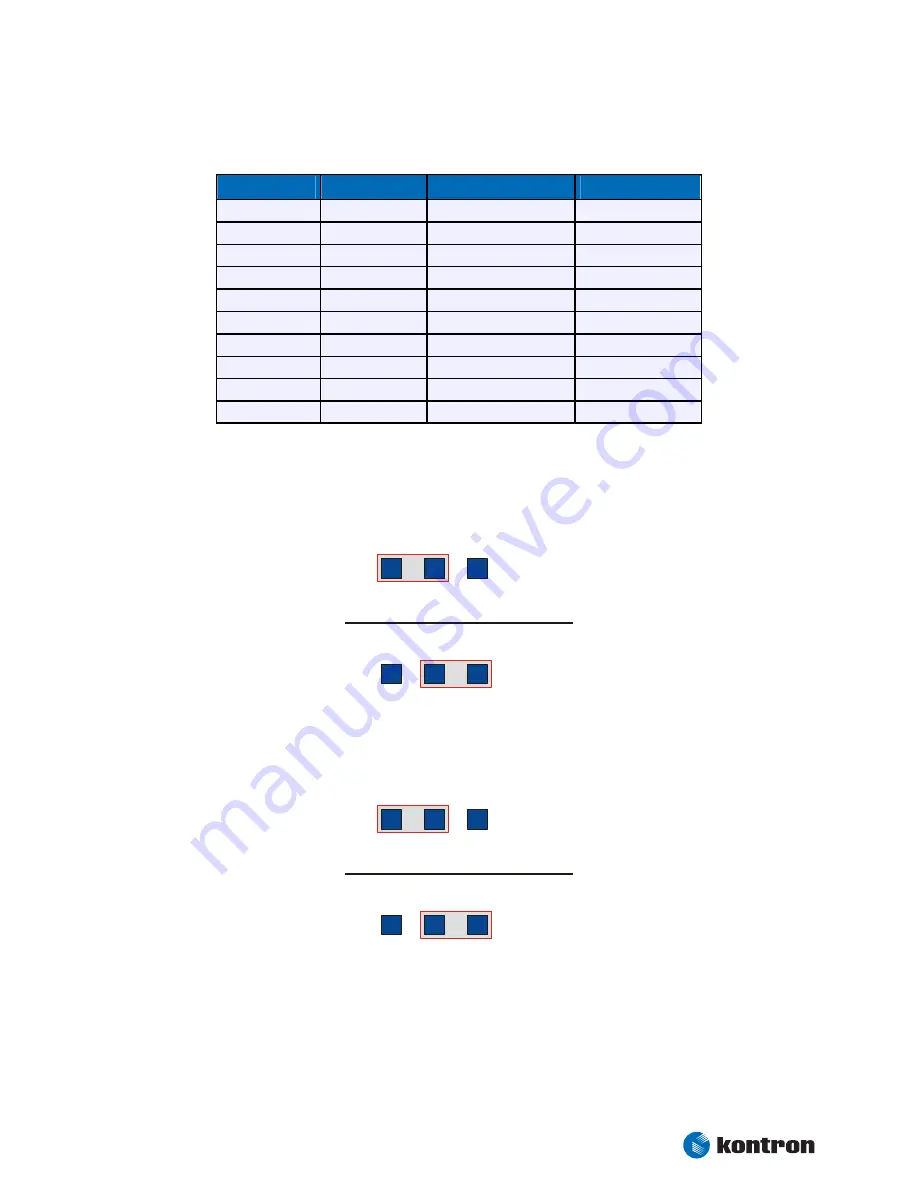
J16 defines two panel power supplies: +5V and +3.3V. 


1

2

3

J16

Panel Vcc = +5V

1

2

3

J16

Panel Vcc = +3.3V


J17 makes it possible to invert the clock signal. 


1

2

3

J17

Normal Clock

1

2

3

J17

Inverted Clock


Summary of Contents for PC/104-520

Page 1: ...Kontron User s Guide PC 104 520 Document Revision 1 2...

Page 2: ...am 8 4 2 Mechanical Specifications 9 4 2 1 PC 104 Bus Connector 9 4 2 2 Module Dimensions 9 4 2 3 Height on Top 9 4 2 4 Height on Bottom 9 4 3 Electrical Specifications 10 4 3 1 Supply Voltage 10 4 3...

Page 3: ...INTERFACE 21 10 1 Connector 21 10 2 Signal Descriptions 22 10 2 1 Example Connection AT keyboard and Other Functions 23 11 PS 2 MOUSE INTERFACE 24 11 1 Connector 24 12 IDE INTERFACE 25 12 1 Connector...

Page 4: ...tensions 41 19 10 1 JIDA BIOS Extension 41 19 10 2 Remote Control Client Extension 41 19 11 Updating the BIOS 43 19 11 1 Flashing a BIOS 43 APPENDIX A SYSTEM RESOURCEN 44 A 1 Interrupt Request Lines 4...

Page 5: ...art of this document may be reproduced transmitted transcribed stored in a retrieval system or translated into any language or computer language in any form or by any means electronic mechanical photo...

Page 6: ...Embedded Modules GmbH that are caused by a faulty Kontron Embedded Modules GmbH product 1 6 Technical Support Technicians and engineers from Kontron Embedded Modules GmbH and or its subsidiaries are a...

Page 7: ...PC 104 form factor The PC 104 520 features the following Industry standard Am5x86 CPU with FPU System ROM BIOS Up to 64 MB SDRAM support Direct memory access DMA controllers Counters Interrupt contro...

Page 8: ...nagement encourages outsourcing of components and technologies to reduce development costs and accelerate product design cycles A need has arisen for a more compact implementation of the PC bus satisf...

Page 9: ...starter kit board Connect the CRT monitor to the CRT interface or a LCD panel to the LCD interface by using the corresponding adapter cable Plug a keyboard to the starter kit s keyboard connector Plu...

Page 10: ...to 64 MB Two Serial Ports COM1 and COM2 RS232C compatible 16550 compatible One Parallel Port LPT1 Bi directional and Enhanced Parallel Port EPP capability IDE Interface P ATA Standard IDE port up to...

Page 11: ...Kontron User s Guide PC 104 520 7 PS 2 Keyboard Controller PS 2 Mouse Controller Watchdog timer WDT Real time Clock requires external battery External ISA Bus Full 8 16 bit Memory and I O access All...

Page 12: ...E Interface BIOS PCI BUS Transformer PC 104 Connector Graphic Controller LynxEM Super I O W83977 PS 2 Interface Serial Ports Parallel Port Floppy Interface LPT FDD COM B COM A Keyboard Mouse SC520 Pro...

Page 13: ...echanical Specifications 4 2 1 PC 104 Bus Connector One 2x32 pin stackthrough and one 2x20 pin stackthrough connector 4 2 2 Module Dimensions 96 x 90mm 3 77 x 3 55 4 2 3 Height on Top Maximum 11 1mm 4...

Page 14: ...e same or equivalent type recommended by the manufacturer Dispose of used batteries according to the manufacturer s instructions Deutsch VORSICHT Explosionsgefahr bei unsachgem em Austausch der Batter...

Page 15: ...mente Sustituya solamente por el mismo o tipo equivalente recomendado por el fabricante Disponga las bater as usadas seg n las instrucciones del fabricante The battery of this product is not considere...

Page 16: ...components are assumed to be operating at a 50 stress level in a 40 C ambient environment and the system is assumed to have not been burned in Manufacturer s data has been used wherever possible The m...

Page 17: ...Microcontroller 32 bit 3 3V PCI bus 5V tolerant Rev 2 2 compliant Integrated SDRAM controller supports 16 64 128 and 256 MBit RAM up to 64 MBytes General Purpose GP bus with programmable timing for 8...

Page 18: ...onnector are defined as C19 and D19 The pinout between PC 104 bus and AT ISA bus is identical between C1 C18 and D1 D18 6 1 1 PC 104 Connectors The PC 104 520 features both XT bus and AT bus extension...

Page 19: ...2 8 VSYNC Vertical sync 14 9 BLUE Analog video blue 3 10 NC Not connected To find the location of the CRT connector on the PC 104 520 board please see the Appendix Connector Layout 7 2 LCD Panel Conne...

Page 20: ...d connect the other end to your display Connect the backlight converter Supply power to your system If no image appears on your display connect a CRT monitor to the CRT connector If you still do not s...

Page 21: ...4h Graphics 1024x768 16 105h Graphics 1024x768 256 111h Graphics 640x480 64K 112h Graphics 640x480 16M 114h Graphics 800x600 64K 115h Graphics 800x600 16M 117h Graphics 1024x768 64K 7 4 3 Panel Config...

Page 22: ...0 FP4 LD1 LD4 B4 BB0 32 FP5 LD5 B5 BB1 13 FP6 LD6 B6 BB2 15 FP7 LD2 LD7 B7 BB3 38 FP8 G0 GA0 40 FP9 G1 GA1 42 FP10 LD3 G2 GA2 44 FP11 G3 GA3 46 FP12 UD0 G4 GB0 48 FP13 UD0 UD1 G5 GB1 34 FP14 UD2 G6 GB...

Page 23: ...DSUB9 2 Part Number 96017 0000 00 0 The fol lowing table shows the pinouts for COMA and COMB as well as necessary connections for DSUB adapters Header Pin Signal Name Function In Out DSUB 25 DSUB 9 1...

Page 24: ...3 PD0 Data 0 I O 2 5 PD1 Data 1 I O 3 7 PD2 Data 2 I O 4 9 PD3 Data 3 I O 5 11 PD4 Data 4 I O 6 13 PD5 Data 5 I O 7 15 PD6 Data 6 I O 8 17 PD7 Data 7 I O 9 19 ACK Acknowledge In 10 21 BUSY Busy In 11...

Page 25: ...ctions of this connector The following table shows the pinout as well as necessary connections for adapters Header Pin Signal Name Function 5 pin DIN Diode 6 pin MiniDIN PS 2 1 Speaker Speaker output...

Page 26: ...is pin However other modules also can use this signal to drive the system speaker KBDAT Keyboard Data Bidirectional I O pin on CPU modules Keyboard data signal KBCLK Keyboard Clock Bidirectional I O p...

Page 27: ...User s Guide PC 104 520 23 10 2 1 Example Connection AT keyboard and Other Functions KBCLK 6 5 DIN41524 6 PIN MINI DIN PS 2 STYLE 5V Vcc 5V Vcc PWRGOOD KBLOCK RESIN BATT Speaker GND KBDAT 3 5 2 1 4 3...

Page 28: ...e following table shows the pinout and connections for a PS 2 mouse adapter Header Pin Signal Name Function 6 pin MiniDIN PS 2 1 MSDAT Mouse data 1 2 VCC 1 5V 4 3 GND Ground 3 1 4 MSCLK Mouse clock 5...

Page 29: ...it by using a mini spacer on the chipDISK hole You also can use a chip DISK adapter chipDISK ADA1 Part Number 96004 0000 00 0 or compact Flash adapter CFC ADA1 Part Num ber 96004 0000 00 2 for more d...

Page 30: ...dix Connector Layout Note 1 To protect the external power lines of peripheral devices make sure that the wires have the right diameter to withstand the maximum available current to enclosure of the pe...

Page 31: ...need an adapter cable which is offered by Kontron KAB PC104520 ETN Part Number 96231 0200 00 0 The following table shows the pinout Header Pin Signal Name Function In Out 1 TXD Transmitter Differentia...

Page 32: ...a slim line 3 5 floppy drive with cable from Kontron FLOPPY MOPS 1 Part Number 96010 0000 00 0 The following table shows the connector pinout Header Pin Signal Name Function Pin Signal Name Function...

Page 33: ...104 520 15 1 Connector The pinout of the power connector P6 8 pins is shown in the table below Header Pin Signal Name Function 1 GND Ground 2 VCC 5V 3 BATT Battery 4 12V 12V 5 NC Not connected 6 12V...

Page 34: ...tional power connectors on addi tional I O cards if your system exceeds the above limitations It is not acceptable to use only the power pins of the PC 104 connector for power supply to the full PC 10...

Page 35: ...n software sourcecode on request or BIOS setup Setup option uses a fixed timeout period of 32 seconds Likewise a JIDA call INT 15h is available Register values AX 0E000h BX 0h Watchdog off BX 1h timeo...

Page 36: ...CK3 for SC520 GPACK1 line use DACK5 DACK6 or DACK7 Place only one jumper for each GPACK0 and GPACK1 line Please select this configuration also in the BIOS setup The delivery default is framed DACK0 DA...

Page 37: ...GPREQ1 line use DREQ5 DREQ6 or DREQ7 Place only one jumper for each GPREQ0 and GPREQ1 line Please select this configuration also in the BIOS setup The delivery default is framed DREQ0 DREQ1 DREQ2 DRE...

Page 38: ...Interface Components LPT Port Components LPT Type Keyboard Interface Components Keyboard Numlock Components Keyboard Repeat PS 2 Mouse Interface Components Enable PS2 Mouse Network Interface PCI ISA...

Page 39: ...tring appears during boot up Press CTRL ALT S to enter SETUP The Main Menu then appears 19 2 General Information The Setup Screen is composed of several sections Setup Screen Location Function Menu Ba...

Page 40: ...Disk C Defines the boot device Enable Watchdog Disabled Enabled Enables or disables the internal watch dog The timeout period is 32 seconds 8Remote Control COM1 COM2 LPT1 Sets the onboard remote port...

Page 41: ...nabled Shows identification strings of ATAPI drives during boot process 19 6 1 Hard Disk x Submenu Feature Option Description Disk Type None Custom Auto ID Custom allows user input for cylinders heads...

Page 42: ...lel port 8LPT Type Standard AT Bidirectional Enhanced Parallel Sets the mode for the parallel port Enable PS2 Mouse Disabled Enabled Enables or disables the PS 2 mouse support in cluding IRQ12 Keyboar...

Page 43: ...cle time I O and memory access 19 8 1 Configure PCI x Submenu Feature Option Description Select IRQ Auto Disabled IRQ5 IRQ9 IRQ10 IRQ11 IRQ15 Defines IRQ of onboard PCI device Auto BIOS selects IRQ Se...

Page 44: ...xt time the system boots the BIOS configures the system ac cording to the Setup selection stored in CMOS Exit No Save OK Cancel Exits Setup without storing in CMOS any new selec tions you may have mad...

Page 45: ...and supports the JIDA 16 bit standard The JIDA 16 bit standard is a software interrupt 15h driven interface for programmers and offers lots of board information functions For detailed information abou...

Page 46: ...R 25 25 GND The SC520Rmt program establish a remote connection Syntax SC520Rmt options P port port COM1 COM4 or LPT1 LPT2 host side F disable host floppy drive K disable host keyboard V disable host g...

Page 47: ...BIOS Use the following procedure to update the BIOS Download the update program from the KONTRON Embedded Modules Website or contact your local technical support for it Use SC520Upd with following ar...

Page 48: ...manufacturer of the add on board and ask about switching to non interrupt sharing Please ensure that the chosen interrupt is not already in use by a PCI device IRQ Use Available Comment 0 Timer0 No 1...

Page 49: ...520 45 A 2 Direct Memory Access DMA Channels DMA Used for Available Comment 0 Yes 1 Yes 2 Floppy No Note 1 3 Yes 4 Cascade No 5 Yes 6 Yes 7 Yes Note 1 If the used for device is disabled in setup the c...

Page 50: ...080 BIOS POST No Fixed 0081 008F DMA Page Register No Fixed 0092 System Control No Fixed 00A0 00BF Interrupt Controller 2 No Fixed 00C0 00DF DMA Controller 2 No Fixed 00E0 00EF System Control No Fixed...

Page 51: ...address the full memory area directly Upper Memory Use Available Comment A0000h BFFFFh VGA Memory No Mainly used by graphic adapter cards C0000h CBFFFh VGA BIOS No Used by onboard VGA ROM CC000h E1FF...

Page 52: ...Guide PC 104 520 48 Appendix B Connector Layout Pin 1 J4 J2 J13 J9 J8 J1 J3 J17 J16 J7 J22 J12 J10 J11 P6 The Board as depicted is a model only showing the positions of the connectors For pincount an...

Page 53: ...26 pos AMP 2 215882 6 or comp KAB DSUB25 1 PN 96015 0000 00 0 for DSUB 25 adaptation J10 PS 2 Mouse Connector 2 54mm 4 pos W P Products 943 12 004 00 or compatible KAB PC104520MOUSE PS2 PN 96230 0200...

Page 54: ...D3 DRQ2 LA19 3 IRQ15 7 SD2 12V LA18 3 NC 8 SD1 NC LA17 3 DACK0 9 SD0 12V MEMR DRQ0 10 IOCHRDY GND 1 MEMW DACK5 11 AEN SMEMW SD8 DRQ5 12 SA19 SMEMR SD9 DACK6 13 SA18 IOW SD10 DRQ6 14 SA17 IOR SD11 DACK...

Page 55: ...2 11 HDD3 FPEN PD4 NC 12 HDD12 GND GND FDIR 13 HDD2 FP6 PD5 NC 14 HDD13 FP19 GND STEP 15 HDD1 FP7 PD6 GND 16 HDD14 FP20 GND WDATA 17 HDD0 FP0 PD7 GND 18 HDD15 FP21 GND WGATE 19 GND FP1 ACK GND 20 KEY...

Page 56: ...ND MSCLK GND 12V 5 KBDAT RED NC 6 KBCLK HSYNC 12V 7 GND GREEN GND 8 VCC 2 VSYNC VCC 2 9 BATT BLUE 10 RESIN NC Note 1 Key pin for PC 104 GND for PC 104 specification 2 To protect the external power lin...

Page 57: ...ineers Programmers and Other Serious PC Users John P Choisser and John O Foster Annabooks 1997 ISBN 0 929392 36 1 C 2 Buses C 2 1 ISA Standard PS 2 Connectors AT Bus Design Eight and Sixteen Bit ISA E...

Page 58: ...hat the modem receives from the telephone line can then be sent to the computer You can search for information about the standard on the Web RS 232 Made Easy Connecting Computers Printers Terminals an...

Page 59: ...ations Second Edition Joe Campbell SAMS 1987 ISBN 0 672 22584 0 Programmer s Guide to the EGA VGA and Super VGA Cards Third Edition Richard Ferraro Addison Wesley 1990 ISBN 0 201 57025 4 The Programme...

Page 60: ...s Guide PC 104 520 56 APPENDIX D REVISION HISTORY Revision Date Edited by Changes 1 0 07 24 2007 M H ttmann First revision 1 1 11 30 2007 M H ttmann Change min operating temperature 1 2 12 05 2007 M H...

Reviews: