background image

www..lairdconnect.com/wireless 

13 

© Copyright 2020  Laird Connectivity. All Rights Reserved 

Americas

: +1-800-492-2320 

Europe

: +44-1628-858-940 

Hong Kong

: +852 2923 0610 


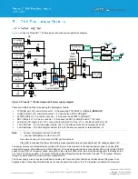
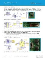
Figure 13: JLINK USB, FTDI USB, and ATMEL SUPPLY switch 

Note:  

We recommend that you use SWD (two-wire interface) to handle future Pinnacle

™ 100 modem firmware upgrades. 

You MUST wire out the SWD (two-wire interface) on your host design (Four lines required: SWDIO [1.8V Logic], 
SWDCLK [1.8V Logic], GND, and VIN (2.2-5.5)].  

M2.60 (P1.00) can be used as SWO (Serial Wire Output) and is not necessary for programming Pinnacle

™ 100 over the SWD 

interface. 

M2.73, nReset_BLE, is not necessary for programming Pinnacle

™ 100 over the SWD interface. 


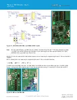
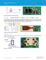
The NRF has a direct USB connection, J10 (NRF USB). The HL7800 also has a direct USB connection, J7 (HL7800 USB). 
Figure 14, shows both USB connectors and J10 must be connected when using J7, to provide 5V to the modem pin M2.9. 


Figure 14: NRF and HL7800 USB 

Summary of Contents for 453-00010-K1

Page 1: ...Version 1 0 ...

Page 2: ...s 2 Copyright 2020 Laird Connectivity All Rights Reserved Americas 1 800 492 2320 Europe 44 1628 858 940 Hong Kong 852 2923 0610 Version Date Notes Contributor s Approver 1 0 22 Jan 2020 Initial Version Mike Richter Jonathan Kaye ...

Page 3: ... 5 3 2 453 00010 Modems 10 5 4 U FL Antenna Attachment DVK 453 00011 K1 Only 10 6 DVK Functional Blocks 11 6 1 Power Supply 11 6 2 NRF Reset Button 12 6 3 SWD Interface 12 6 4 NRF and HL7800 USB 13 6 5 DVK Disconnect Switches 14 6 6 I O Headers Disconnect 14 6 7 M2 Pins P1 Headers and DIP Switch Interconnection 15 6 8 PinnacleTM 100 UART Mapping 17 6 9 Indicator LEDs 18 6 10 Push Buttons 19 6 11 B...

Page 4: ...al antenna All kits contain the following items Development Board The development board with the Pinnacle 100 Modem contains CON1 which is used to attach the PinnacleTM 100 modem and is held in place by screws Hardware Two M2 Screws to secure modem Four Plastic Standoffs and nuts Power Options USB cable Type A to micro type B DC power jack for external power supply 12 VDC max AA or AAA battery pac...

Page 5: ...ring the development board USB micro USB type B External DC supply 4 4 12V supplied Center positive barrel connector or header for bench supply 4 AA batteries not supplied Assume Lithium Iron Disulfide 4 4 7 2V 2 AA batteries not supplied Assume Lithium Iron Disulfide 2 2 3 6V When powering the DVK with USB Ext DC or 4 AA a DC DC converter is used to supply the DVK with 3 7V The DVK also includes ...

Page 6: ...www lairdconnect com wireless 6 Copyright 2020 Laird Connectivity All Rights Reserved Americas 1 800 492 2320 Europe 44 1628 858 940 Hong Kong 852 2923 0610 Figure 1 Dev board contents and locations ...

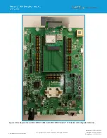
Page 7: ...7 Copyright 2020 Laird Connectivity All Rights Reserved Americas 1 800 492 2320 Europe 44 1628 858 940 Hong Kong 852 2923 0610 Figure 2 Development board 453 00010 K1 fitted with 453 00010 Pinnacle 100 modem with integrated antenna ...

Page 8: ...g Kong 852 2923 0610 Note To ensure correct out of the box configuration the Pinnacle 100 development board switches must be configured as shown in Figure 3 The default recommend power connection is USB with FTDI USB J30 connected Figure 3 Default Pinnacle 100 development board 453 00010 K1 jumper and switch settings image for 453 00010 ...

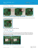
Page 9: ... metal edge arrow 1 shown in Figure 5 grab the edge of the SIM card arrow 2 and pull out Figure 5 Removing nano SIM from PinnacleTM 100 modem Place the modem into CON1 and use the two provided M2 screws to thread into the standoffs to hold the modem down Both screws must be securely tightened to the modem and standoffs for proper modem operation The standoffs provide additional RF grounding for th...

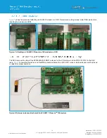
Page 10: ...s in the PCB holes before inserting the modem into CON1 Figure 7 Attaching a 453 00010 PinnacleTM 100 modem to a DVK The DVK comes with a Revie Flex EFF6925A3S 15MHF1 antenna for the LTE radio and a FlexPIFA 001 0014 for the BLE radio Figure 8 shows the Revie Flex and FlexPIFA antennas attached to a 453 00011 modem Both antennas must be placed on plastic for proper operation Figure 8 External ante...

Page 11: ...rnal DC supply 4 4V 12V connected to either the DC Plug J17 or the Bench connector J6 4 x AA batteries Four AA Energizer Lithium 4 4 7 2V batteries connected to terminal block J22 2 x AA batteries Two AA Energizer Lithium 2 2 3 6V batteries connected to terminal block J2 Note Connect USB cables to both J18 and J30 Connect USB cables to both J7 and J10 Recommend using a 1A or above for USB port con...

Page 12: ...ment kit reset button Figure 11 NRF reset schematic and routing through DIP switch S1 10 AND gate The development board provides two options for connecting to the modem s SWD interface the signals SWDIO SWDCLK and SWO are switched by U10 based on the position on SW13 DEBUG SELECT External header J14 allows an external SWD debugger programmer to be connected to the modem The DEBUG SELECT SW13 must ...

Page 13: ...terface on your host design Four lines required SWDIO 1 8V Logic SWDCLK 1 8V Logic GND and VIN 2 2 5 5 M2 60 P1 00 can be used as SWO Serial Wire Output and is not necessary for programming Pinnacle 100 over the SWD interface M2 73 nReset_BLE is not necessary for programming Pinnacle 100 over the SWD interface The NRF has a direct USB connection J10 NRF USB The HL7800 also has a direct USB connect...

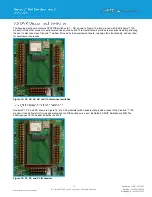
Page 14: ...lity is provided to maximize flexibility allowing the user to disconnect any Pinnacle modem I O used by the development board re assign their functionality and use them for development purposes Figure 15 S1 S2 S3 S4 and S5 disconnect switches Headers P1 P2 and P3 shown in Figure 16 are 2 54 millimeter pitch headers that provide access to the Pinnacle 100 modem I O and allows for IO re assignment w...

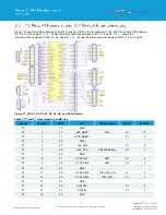
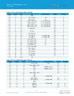
Page 15: ...tween CON1 P2 S2 and S5 Table 3 shows the interconnections between CON1 P3 S3 and S4 Figure 17 M2 P1 P2 P3 S1 S2 S3 S4 and S5 schematic Table 1 P1 and S1 signal mapping to M2 pins Header Position M2 Net DVK Function Switch Position P1 1 75 GND P1 2 73 nBT_REST SW5 S1 10 P1 3 71 nLTE_RESET S1 9 P1 4 69 GND P1 5 67 1V8_SIM S1 8 P1 6 65 BAT_RTC CR2032 Battery S1 7 P1 7 63 GND P1 8 61 P0 03_AIN1 SW2 S...

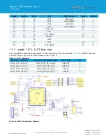
Page 16: ...USB_D J7 HL7800 USB S5 12 P2 13 50 HL_USB_D J7 HL7800 USB S5 11 P2 14 52 LTE_UART0_RX J11 S5 10 P2 15 54 LTE_UART0_RTS J11 S5 9 P2 16 56 LTE_UART0_CTS J11 S5 8 P2 17 58 LTE_UART0_TX J11 S5 7 P2 18 60 P1 00_TRC0_SWO S5 6 P2 19 62 P0 12_TRC1 S5 5 P2 20 64 P0 11_TRC2 S5 4 P2 21 66 P1 09_TRC3 S5 3 P2 22 68 P1 11_VGPIO S5 2 P2 23 70 nPWR_ON S5 1 P2 24 72 74 VIN Table 3 P3 S3 and S4 signal mapping to M2...

Page 17: ... S3 7 P3 22 37 SIM_RST S3 8 39 GND P3 23 41 P1 01 S3 9 P3 24 43 P1 08_GPIO2 S3 10 The 4 wire UART connections on the Pinnacle 100 modem and the FTDI IC are shown in Table 4 The UART connections schematic shown in Figure 18 and DVK locations shown in Figure 19 Table 4 UART connections Pinnacle 100 M2 U5 Pinnacle 100 Default Function FTDI IC UART J12 M2 38 P0 07 U5 pin 32 HOST_UART_RTS output USB_RT...

Page 18: ...00 as indicated in Table 5 The Schematic and location are shown in Figure 20 Table 5 PinnacleTM 100 DVK LEDs and signal mapping Designator Color NRF Port Name LED1 Blue P1 04 LED2 Green P1 05 LED3 Red P1 06 LED4 Green P1 07 Note The PinnacleTM 100 connections to the LEDs can be removed by switching positions 2 3 4 and 5 of S3 to the OFF position LED4 indicate the status of the bootloader LED5 Red ...

Page 19: ... M2 23 P0 04 SW4 M2 59 P0 02 Note The PinnacleTM 100 connections to the buttons can be removed by switching the positions of the DIP switches S4 Position 1 SW1 S1 Position 6 SW2 S3 Position 6 SW3 and S1 Position 5 SW4 to the OFF position SW1 is used by the bootloader to enter UART mode so that must be considered if a user wants to use it for another purpose Figure 21 Push button schematic The deve...

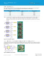
Page 20: ...ments using modem pin M2 53 P0 29 shown in Figure 23 Figure 23 VIN monitor schematic The DVK includes a GPS antenna shown in Figure 24 that is connected to the modem using J23 and a U FL to U FL cable Figure 24 GPS antenna Figure 25 shows a removable jumper on J4 which is provided to break the power supply line directly to the modem allowing the measurement of the PinnacleTM 100 current consumptio...

Page 21: ...Pinnacle 100 modem NFC circuit uses two pins M2 22 NFC1 and M2 20 NFC2 to connect the antenna C37 300pF and C38 300pF are RF tuning elements for the flexi PCB NFC antenna Turning OFF S2 Position 9 and 10 to disconnect J16 and the RF tuning elements Figure 26 shows the NFC schematic and location on the DVK Figure 26 J16 NFC connector schematic Placing a CR2302 battery into connector J13 shown in Fi...

Page 22: ...0 A 3 3V to 1 8V level shifter is available for users J8 can be removed if a different voltage is required Figure 28 U9 Level Shifter By disconnecting DIP switches S2 5 6 7 8 then connecting jumpers from J11 Pin 2 to J12 Pin 2 J11 Pin 4 to J12 Pin 4 J11 Pin 5 to J12 Pin 5 J11 Pin 6 to J12 Pin 6 The USB UART can be connected to the HL7800 Debug port instead ...

Page 23: ... evaluation process and ultimately into mass production Additional documentation can be accessed from the Documentation tab of the Laird Pinnacle 100 Product Page For any additional questions or queries or to receive technical support for this Development Kit or for the Pinnacle 100 modem please contact Embedded Wireless Solutions Support https www lairdconnect com resources support Copyright 2020...

Reviews: