https://www.lairdconnect.com/wireless-
modules/bluetooth-modules
11
© Copyright 2019 Laird. All Rights Reserved
Americas
: +1-800-492-2320
Europe
: +44-1628-858-940
Hong Kong
: +852 2923 0610
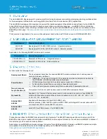
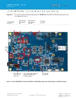
Table 1: Dev board power sources and switch positions
Selection Switch SW7 Position/Source/
Voltage Operating Mode
Dev Board Power Supply Switch Positions
SW5 default and only
position
3V3
Position 1V8 not valid for
DVK-BL654PA
SW8 default and
only 5V5_AAA
Position 2V5 not
valid for DVK-
BL654PA
Connect USB
cable into
USB3
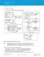
Present selected voltage to the BL654PA pin
BL654PA VDD pin
BL654PA VDD_HV
pin
BL654PA
VBUS pin
SW7 top position
Source:
USB3
Operating Mode:
High
voltage using BL654PA
USB (USB3)
USB3 voltage
USB3 voltage
SW7 middle position
Source:
Operating Mode:
Normal
voltage
Decided by SW5
(default and only
SW5 position is
3V3
)
N/A
N/A
SW7 bottom position
Source:
SW8
Operating Mode:
High
voltage
Note 1
Decided by SW8
(default and only
SW8 position
5V5_AAA
DVK-
BL654PA)
N/A
Power Source and Switch Location Notes:
Note 1:
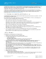
No voltage is presented to VDD pin, as in High voltage mode, the VDD pin becomes an output voltage pin. It can
be used to supply external circuitry from the VDD pin. Before any current can be taken from the BL654PA VDD
pin, this feature must be enabled in the BL654PA. Additionally, the VDD output voltage is configurable from 1.8V
to 3.3V with possible settings of 1.8V, 2.1V, 2.4V, 2.7V, 3.0V, and 3.3V. The default voltage is 1.8V.
Note 2:
SW6 default and valid position is
3V3/1V8
. SW6 position
coin cell
is not valid for BL654PA and therefore coin
cell power supply option operation of the BL654PA module is not possible (J34 coin cell holder cannot be used
Summary of Contents for 455-00022
Page 1: ...Version 1 0 ...


