https://www.lairdconnect.com/wireless-
modules/bluetooth-modules
12
© Copyright 2019 Laird. All Rights Reserved
Americas
: +1-800-492-2320
Europe
: +44-1628-858-940
Hong Kong
: +852 2923 0610
on the DVK-BL654PA). Therefore, if SW6 is accidentally set to the
coin cell
position, then the voltage selected
with SW5 (default position 3V3) is not presented to the BL654PA.
Note:
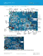
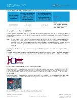
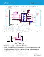
The development board for BL654PA has on-board circuitry to allow access to BL654PA SWD interface (via USB
connector USB2). Use USB2 only to power the development board when BL654PA SWD interface is needed. Refer
to
. When USB2 is used, USB1 does not need to be used for DC power.
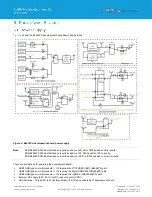
The development board power supply circuitry
’s special feature is that it resolves whether the BL654PA VDD pin is an input
supply pin (in Normal Voltage mode) or becomes an output supply voltage pin (in High Voltage mode).
On the development board, the power circuity net names are as follows:
▪
VCC_3V3
– Supplies regulated 3.3V power to the FTDI chip as well as temperature sensor (U1).
▪
VSUPPLY
– Supplies regulated 3.3V (3V3) or 1.8V (1V8) via selection switch SW5 to net VSUPPLY which is connected
to input of Load switch U21. For the DVK-BL654PA, the default and only valid SW5 position is 3V3.
▪
VCC_2V5_5V5
– Selection switch SW8 supplies either regulated 2.5V (
2V5
) or 3x AAA (
5V5_AAA
) battery voltage
(4.5V) can be used for when BL654PA is powered in High Voltage mode (using the VDD_HV pin). For the DVK-
BL654PA, the default and only valid SW8 position is
5V5_AAA
.
▪
V5V
– The main development board power supply’s buck-boosted output (that is 5V) supplies a discrete regulator made
up of Q3 and U19. U19 OpAmp drives Q3 to generate regulated voltage (that then is connected to input of load switch
U20) that tracks control signal VDD_nRF_SENSE.
▪
VDD_VSRC_nRF
– Supplies the FTDI chip IO and all other sensors and circuitry. VDD_VSRC_nRF is generated from
load switches U20 or U19.
▪
VDD_nRF_SENSE
– Used as control signal to drive control pin of load switches U20 and U19. The source of
VDD_nRF_SENSE is the BL654PA VDD pin. When BL654PA is powered in High Voltage mode (using the VDD_HV pin),
the BL654PA VDD pin becomes an output.
▪
VDD_nRF_SW
– Selection switch SW6 supplies either VDD_SRC_nRF or coin cell (J34). When the BL654PA operates
in Normal Voltage mode (SW7 in middle position and voltage source is either 1.8V or 3.3V selected by SW5). Also
supplies the I2C RTC chip (U16). The use case for powering this is that the RTC chip can be configured so that, after the
pre-determined time, the RTC chip outputs (via RTC_ALARM pin) a transition level that can be used to wake up the
BL654PA module from deep sleep.
▪
VDD_nRFp
– Supplies the BL654PA series module only. Current measuring block on the development board only
measures the current into power domain VDD_nRFp (that is current going into header J7 pin 1).
▪
VDD_nRF
– Supplies the BL654PA series module only and is to the current that has come out of the current measuring
block on the development board on header connector J7 pin 2.
▪
VDD_HVp
– Supplies the BL654PA series module only. Current measuring block on the development board only
measures the current into power domain VDD_nRFp (that is current going into header J9 pin1).
▪
VDD_HV
– Supplies the BL654PA series module only and is to the current that has come out of the current measuring
block on the development board on header connector J9pin2.
▪
VBUS_nRFp
– This voltage from USB cable plugged into connector USB3, that is directly fed to BL654PA VBUS pin (via
0R resistor R50) on net VBUS_nRF.
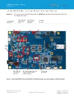
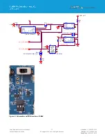
TIP:
Operating the development board at 75°C or above causes issue related to Q2 (it starts turning on) which results in
VDD_VSRC_nRF supplying heading towards 0V or turning off. To overcome this temperature issue, bridge with solder
the open-solderbridge SB24 which connects 1MOhms resistor to ground onto the gate of Q2.
The 1-MOhm resistor results in extra current consumption of (= VDD_nRF_SENSE/1Mohms) added to any current
measurements made when operating the BL654PA module on devboard in High voltage mode (VDD_HV pin) ONLY
which is when SW7 in Top position or Bottom position (and in that case by default VDD_nRF_SENSE is 1.8V).
shows PCB location of SB24 and schematic showing SB24.
Summary of Contents for 455-00022
Page 1: ...Version 1 0 ...


