BL652 Development Kit
User Guide
Embedded Wireless Solutions Support Center:
http://ews-support.lairdtech.com
www.lairdtech.com/bluetooth
34
© Copyright 2016 Laird. All Rights Reserved
Americas: +1-800-492-2320
Europe: +44-1628-858-940
Hong Kong: +852 2923 0610
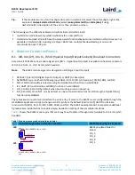
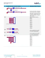
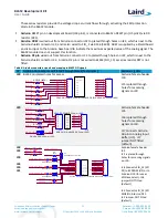
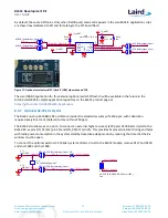
Figure 18: Optional external 32.768kHz crystal circuit schematic and PCB
A smartBASIC application will be available in the future in the GitHub smartBASIC sample application repository
on the BL652 product page at
http://www.lairdtech.com/products/bl652-ble-module
9
O
THER
F
EATURES
9.1
Current Consumption Measurement
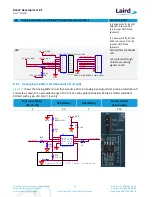
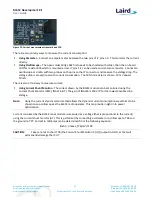
A removable jumper (on J7) is provided to break the power supply line directly to the module, allowing you to
measure current consumption. For normal operation, the jumper on J7 between pin1 and pin2 must be fitted
(and is fitted by default).
IMPORTANT: To achieve the optimal power consumption of the BL652 series module on the development
board, see the “LowPower.sb” file in the GitHub smartBASIC sample application repository on the
BL652 product page at
https://github.com/LairdCP/BL652-Applications
.
Note:
This measures the current consumption of the BL652 series module ONLY.
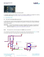
The current drawn by the BL652 series module can be monitored on the development board.
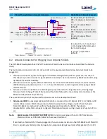
Figure 19
shows
the schematic and location of measuring points on the PCB related to current measurements.
C17
0.1uF,16V
VCC_Radio
TP6
NOPOP (TH_TEST_POINT)
1
R52
0R
R53
0R
GND
TP5
NOPOP (TH_TEST_POINT)
1
TP7
NOPOP (TH_TEST_POINT)
1
GND
GND
GND
R47 NOPOP (0R)
U7
CurrentShuntMonitor,200V/V
IN
+
A1
IN
-
A2
GN
D
B1
OU
T
B2
I(mA)=(Vmeas(mV)/100
R54
1R,1%
R56
1R,1%
J7 jumper fitted (Default)
R30
NOPOP (3R3,1%)
SB2
NOPOP (Solderbridge_Open)
1
1
2
2
R76
10R,1%
SB1
NOPOP (Solderbridge)
1
1
2
2
PIN HEADER,2.54mm 1X2P
J7
1
1
2
2
VCC_BLE
VCC_Radio


