SDC-CF10G
Hardware Integration Guide
Embedded Wireless Solutions Support Center:
http://ews-support.lairdtech.com
www.lairdtech.com/wireless
10
Americas: +1-800-492-2320
Europe: +44-1628-858-940
Hong Kong: +852 2923 0610
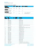
Recommended Operating Conditions
Parameter
Min.
Typical
Max.
Units
Comments
Supply Voltage
VDDIO, VDDBUS
VDDCORE, PLLVDD, AVDD
3.0
1.71
3.3
1.8
3.6
1.89
V
V
Logic Inputs
V
INH
, Input High Voltage
V
INL
, Input Low Voltage
2.0
–
–
–
–
0.8
V
V
Logic Outputs
V
OH
, Output High Voltage
V
OL
, Output Low Voltage
2.4
–
–
–
–
0.4
V
V
Current is determined
by the specific pad.
P
IN
D
EFINITIONS
Pin
Number
Pin
Name
I/O
Power
Type
Description
1
GND
Ground
2
Slot0_data3
Data bus, bit 3
3
Slot0_data4
Data bus, bit 4
4
Slot0_data5
Data bus, bit 5
5
Slot0_data6
Data bus, bit 6
6
Slot0_data7
Data bus, bit 7
7
Slot0_nCE1
Enable for even-numbered address bytes.
Active low.
8
Slot0_addr10
Address bus, bit 10
9
Slot0_nOE
I
Memory access output enable. Active low.
10
Slot0_addr9
Address bus, bit 9
11
Slot0_addr8
Address bus, bit 8
12
Slot0_addr7
Address bus, bit 7
13
VCC3_3
3.3V Module Power
14
Slot0_addr6
Address bus, bit 6
15
Slot0_addr5
Address bus, bit 5
16
Slot0_addr4
Address bus, bit 4
17
Slot0_addr3
Address bus, bit 3
18
Slot0_addr2
Address bus, bit 2
19
Slot0_addr1
Address bus, bit 1
20
Slot0_addr0
Address bus, bit 0
21
Slot0_data0
Data bus, bit 0
22
Slot0_data1
Data bus, bit 1
23
Rfu_data2
Data bus, bit 2
24
Slot0_nIOIS16
Current access is 16 bit. Active low.
25
Slot0_nCD2
Card detect. Tied to ground in module.


