LoRa/BLE Modules
Hardware Integration Guide
Embedded Wireless Solutions Support Center:
http://ews-support.lairdtech.com
www.lairdtech.com/wireless
27
© Copyright 2016 Laird. All Rights Reserved
Americas: +1-800-492-2320
Europe: +44-1628-858-940
Hong Kong: +852 2923 0610
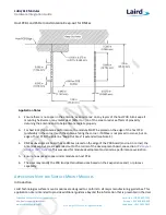
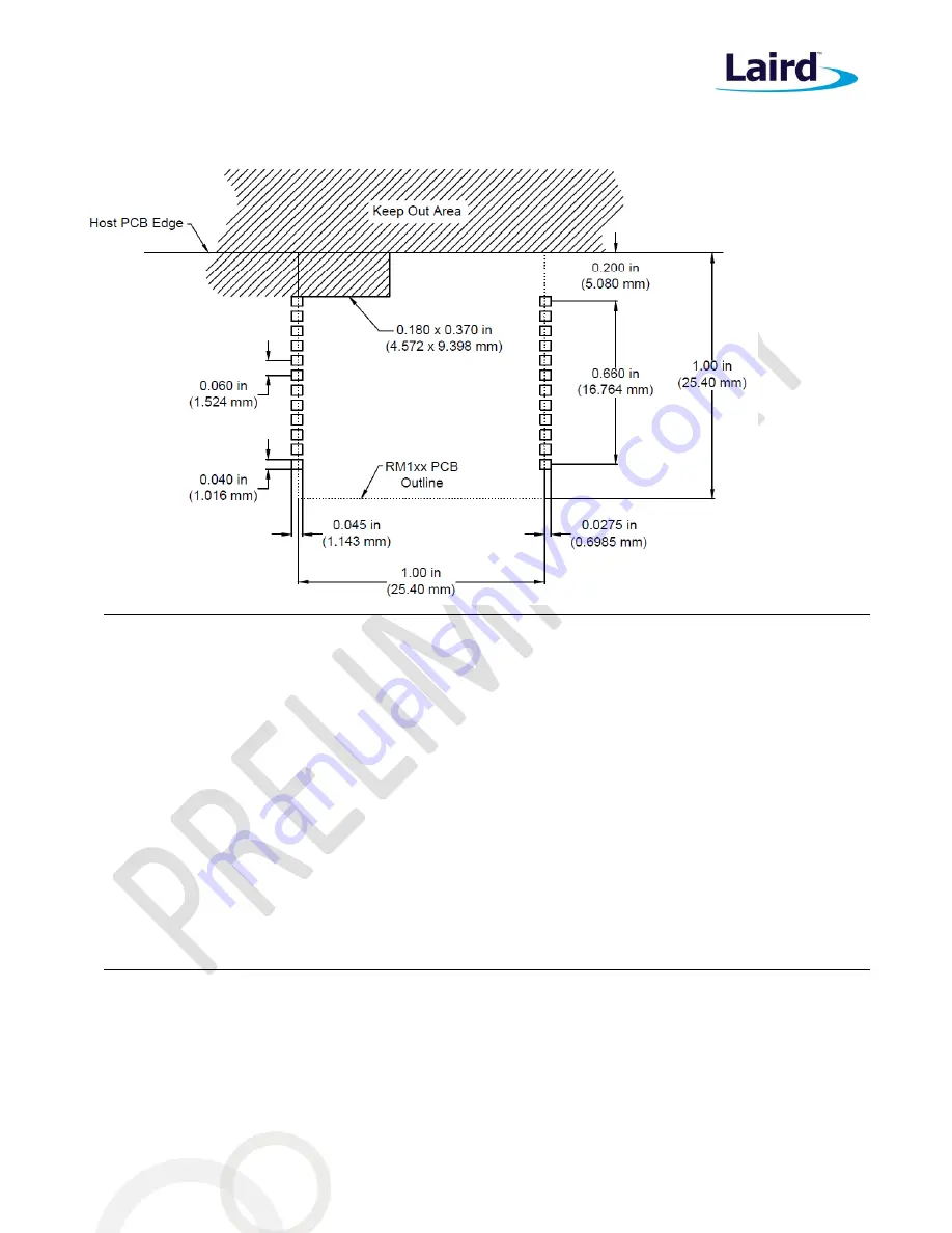
Host PCB Land Pattern and Antenna Keep-out for RM1xx
Application Notes
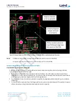
1. Ensure there is no copper in the antenna ‘keep out area’ on any layers of the host PCB. Also keep all
mounting hardware or any metal clear (Refer to
) on of the area to reduce effects of proximity
detuning the antenna and to help antenna radiate properly.
3. For best BLE chip antenna performance, the module MUST be placed on the edge of the host PCB
(preferably in the corner) with the antenna facing the corner. If RM1xx is not placed in corner, but on
edge of host PCB, the antenna “Keep Out Area” is extended (see Note 4).
4. RM1xx development board has an RM1xx placed on the edge of the PCB board (and not in corner) the
Antenna keep out area is extended out to the corner of the development board, see section
. This was used for module development and antenna performance evaluation.
5. Ensure no exposed copper under module on host PCB.
6. The user may modify the PCB land pattern dimensions based on their experience and / or process
capability.
A
PPLICATION
N
OTE FOR
S
URFACE
M
OUNT
M
ODULES
Introduction
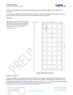
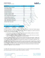
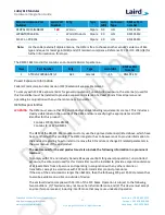
Laird Technologies surface mount modules are designed to conform to all major manufacturing guidelines. This
application note is intended to provide additional guidance beyond the information that is presented in the User


