LoRa/BLE Modules
Hardware Integration Guide
Embedded Wireless Solutions Support Center:
http://ews-support.lairdtech.com
www.lairdtech.com/wireless
24
© Copyright 2016 Laird. All Rights Reserved
Americas: +1-800-492-2320
Europe: +44-1628-858-940
Hong Kong: +852 2923 0610
PCB Layout on Host PCB - General
Checklist (for PCB):
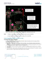
MUST locate RM1xx module close to the edge of PCB (mandatory for RM1xx for on-board chip antenna
to radiate properly).
Use solid GND plane on inner layer (for best EMC and RF performance).
All module GND pins MUST be connected to host PCB GND.
Place GND vias close to module GND pads as possible.
Unused PCB area on surface layer can be flooded with copper but place GND vias regularly to connect
copper flood to inner GND plane. If GND flood copper exists on the top PCB layer (under of the RM1xx
module), then connect with GND vias to inner GND plane and ensure that it is covered with solder mask.
Route traces to avoid noise being picked up on VCC supply and AIN (analogue) and SIO (digital) traces.
Ensure no exposed copper beneath the module (refer to land pattern of RM1xx development board).
Antenna Keep-out on Host PCB
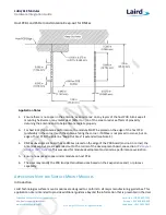
Ensure there is no copper in the antenna keep-out area on any layers of the host PCB. Keep all mounting
hardware and metal clear of the area to allow proper antenna radiation.
For best antenna performance, place the RM1xx module on the edge of the host PCB, preferably in the
corner with the antenna facing the corner.
The RM1xx development board has the RM1xx module on the edge of the board (not in the corner).
The antenna keep-out area is defined by the RM1xx development board which was used for module
development and antenna performance evaluation is shown in
, where the antenna keep-out
area is composed of PCB dielectric (no copper) sitting under the RM1xx antenna.
A different host PCB thickness dielectric will have small effect on antenna.
The antenna-keep-out defined in
Host PCB Land Pattern and Antenna Keepout
is placed in the corner of the host PCB. When RM1xx-SM cannot be placed as such, it must be placed on
the edge of the host PCB and the antenna keep out must be observed. An example is shown in

