Laird MSD45N
Hardware Integration Guide, version 1.1
Embedded Wireless Solutions Support Center:
http://ews-support.lairdtech.com
www.lairdtech.com/wireless
9
Laird Technologies
Americas: +1-800-492-2320 Option 2
Europe: +44-1628-858-940
Hong Kong: +852-2268-6567 x026
SDIO Timing Requirements
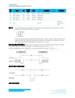
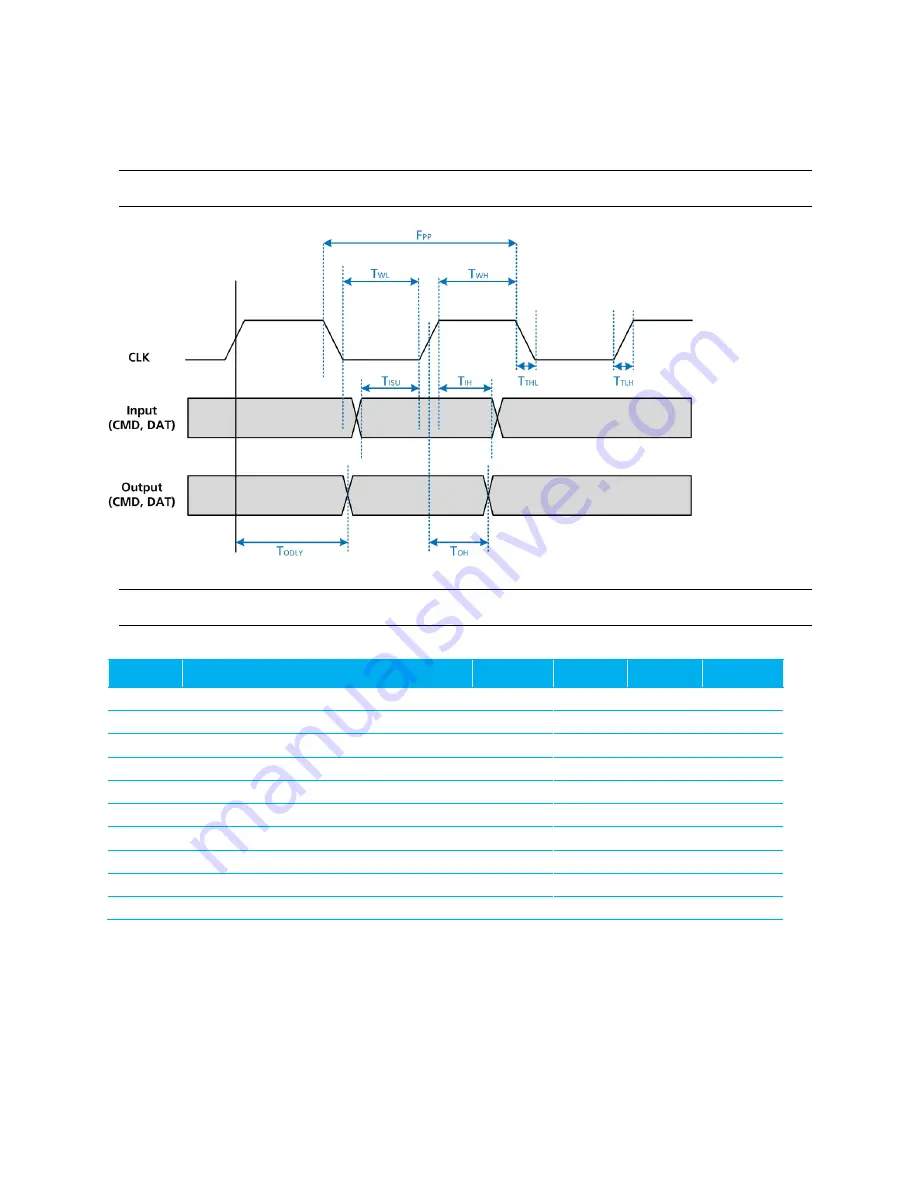
The following figure (Figure 1) and table display SDIO default mode timing.
Note: The SDIO bus should not exceed a 25 MHz clock rate.
Figure 2: SDIO Default Mode Timing
Note: Timing is based on CL
≤
40 pF load on CMD and Data.
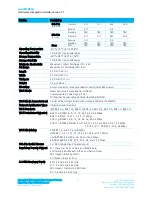
Table 4: SDIO Timing Requirements
Symbol
Parameter
Min.
Typ.
Max.
Unit
fPP
Frequency – Data Transfer mode
0
-
50
MHz
tWL
Clock low time
7
-
-
ns
tWH
Clock high time
7
-
-
ns
tTLH
Clock rise time
-
-
10
ns
tTHL
Clock low time
-
-
10
ns
Inputs: CMD, DAT (referenced to CLK)
tISU
Input setup time
6
-
-
ns
tIH
Input hold time
2
-
-
ns
Outputs: CMD, DAT (referenced to CLK)
tODLY
Output delay time – Data Transfer mode
0
-
14
ns


