background image

https://www.lairdconnect.com/vela-if820-series


17 

© Copyright 2023 Laird Connectivity. All Rights 

Reserved 

https://www.lairdconnect.com/contact


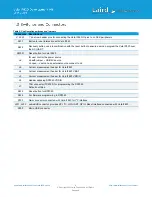
A MikroE connector is connected to Vela IF820 and is reserved for user programming. Mapping table is shown as below. 

Table 5: J202 Pin Map 

Header Connector 

Connector.pin 

MikroE pre-

defined function 

Note 


J202.1 

GPIO 

Jumper should be installed in: 


MHF4 variant : J3 pin 3-4 


Antenna variant : J3 pin 7-8 

J202.2 

GPIO 

Jumper should be installed in: 


MHF4 variant : J1 pin 13- 14 


Antenna variant : J2 pin 21-22 

J202.3 

P_UART_RXD 

Jumper should be installed in: 


MHF4 variant : J2 pin 19- 20 


Antenna variant : J1 pin 19- 20 

J202.4 

P_UART_TXD 

Jumper should be installed in:  


MHF4 variant : J2 pin 17-18 


Antenna variant : J1 pin 23-24 

J202.5 

I

2

C_CLK 

Jumper should be installed in: 


MHF4 variant : J1 pin 5-6 


Antenna variant : J2 pin 19-20 

J202.6 

I

2

C_DATA 

Jumper should be installed in: 


MHF4 variant : J2 pin 13-14 


Antenna variant : J3 pin 3-4 


J202.7 

5V 


J202.8 

GND 


Table 6: J201 Pin Map 

Header Connector 

Connector 

Pin 

MikroE pre 

defined function 

note 


J201.1 

GPIO 

Jumper should be installed in 


MHF4 variant : J1 pin 15 -16 


Antenna variant : J1 pin 3 - 4 

J201.2 

RST_L 

Jumper should be installed in 


MHF4 variant : J2 pin 23 

– 24 


Antenna variant : J3 pin 5 

– 6 

J201.3 

SPI_CS 

Jumper should be installed in 


MHF4 variant : J1 pin 11 

– 12 


Antenna variant : J1 pin 1 

– 2 

J201.4 

SPI_SCK 

Jumper should be installed in  


MHF4 variant  : J1 pin 19 

– 20 


Antenna variant : J1 pin 9 

– 10 

J201.5 

SPI_MISO 

Jumper should be installed in 


MHF4 variant : J1 pin 21 

– 22 


Antenna variant : J1 pin 11 

– 12 

J201.6 

SPI_MOSI 

Jumper should be installed in  


MHF4 variant  : J1 pin 23 

– 24 


Antenna variant : J1 pin 15 

– 16 

J201.7 

VDDIO 

3.3V by default  


J201.8 

GND 


Summary of Contents for Vela IF820

Page 1: ...Version 1 0...

Page 2: ...eries 2 Copyright 2023 Laird Connectivity All Rights Reserved https www lairdconnect com contact Version Date Notes Contributors Approver 1 0 19 Sept 2023 Initial Release Louis Chang Rikki Horrigan Ry...

Page 3: ...nderstanding the Development Board 8 4 3 Switches and Connectors 9 4 4 Dual row 2 54 mm pitch pin headers 10 5 Functional Blocks 12 5 1 Power Architecture 12 5 2 Programming the RP2040 Firmware 13 5 2...

Page 4: ...he Vela IF820 mounted on the development board This document covers a description and design examples of the Vela IF820 DVK board and its features The following documents are available from the Vela I...

Page 5: ...5V which may be provided by either microUSB or an external source connected to specific pin header Module VBAT 3 3V which may be provided a specific external pin header or microUSB Module VDDIO 3 3V...

Page 6: ...idge External UART Source using J2 pin 1 3 5 7 9 11 comply with FTDI cable USB to TTL 232 after development board already powered On board 3v3 supplied from either USB 5V or reserved External pin head...

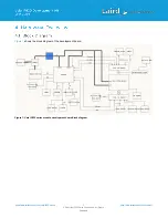
Page 7: ...a if820 series 7 Copyright 2023 Laird Connectivity All Rights Reserved https www lairdconnect com contact Figure 1 shows the block diagram of the development board Figure 1 Vela IF820 series module de...

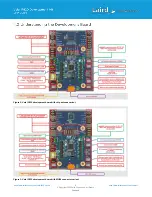
Page 8: ...f820 series 8 Copyright 2023 Laird Connectivity All Rights Reserved https www lairdconnect com contact Figure 2 Vela IF820 development board with chip antenna variant Figure 3 Vela IF820 development b...

Page 9: ...T SW301 Reset button for Vela IF820 J6 for user control the power source J6 with jumper USB 5V source J6 open user can use external source connect to J6 J9 Current measurement header for Vela IF820 J4...

Page 10: ...nnector connector pin connect to IF820 pin number IF820 Module pre defined function Install jumper to work with J1 2 1 BT_DEV_WAKE RP2040 J1 4 2 BT_HOST_WAKE RP2040 J1 6 4 I2 C_CLK MikroE socket and Q...

Page 11: ...J1 18 14 P_UART_CTS RP2040 J1 20 15 P_UART_RXD RP2040 J1 22 16 P_UART_RTS RP2040 J1 24 17 P_UART_TXD RP2040 J2 1 no GND no J2 3 24 BT_UART_RTS RP2040 J2 5 no empty no J2 7 26 BT_UART_RXD RP2040 J2 9 2...

Page 12: ...rtions and the VBAT source provides power for all other radio needs The DVK provides 3 3V power for both VDDIO and VBAT by a 5V to 3 3V on board regulator 5V input can be either supplied from Micro US...

Page 13: ...he board in some way To do so unplug and then reconnect the USB connector or press the RP2040 reset button if one is available Once in BOOTSEL mode the user should see a USB storage device show up on...

Page 14: ...ela IF820 mapping to P0 of the CY20820 chipset Pressing this button grounds this pin Please see the GPIO pin numbers of the different Vela IF820 module variants in the table below Header Connector MHF...

Page 15: ...oots Flashes blue for UART0 HCI TX and RX Flashes red for UART1 EZ Serial TX and RX Flashes green for USB DAP debugger commands Schematic MHF4 variant Antenna variant note Vela IF820 pin 5 P4 of CYW20...

Page 16: ...is shown as below Header Connector Connector pin Qwiic pre defined function Note P202 1 GND P202 2 VDDIO 3 3V by default P202 3 I2 C DATA jumper should be installed in MHF4 variant J2 pin 13 14 Antenn...

Page 17: ...J202 5 I2 C_CLK Jumper should be installed in MHF4 variant J1 pin 5 6 Antenna variant J2 pin 19 20 J202 6 I2 C_DATA Jumper should be installed in MHF4 variant J2 pin 13 14 Antenna variant J3 pin 3 4 J...

Page 18: ...d https www lairdconnect com contact Figure 12 MikroE connector Please note P UART function of MikroE connector is workable after hardware version 4 0 checked by reviewing silkscreen on the backside o...

Page 19: ...se P UART function working with MikroE device please cut the solder bridge between Vela IF820 and RP2040 for any interference prevented Figure 14 Solder bridge connects Vela IF820 and RP2040 The Vela...

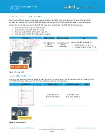
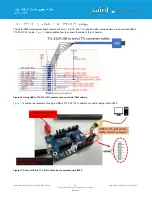
Page 20: ...7 9 and 11 to enable USB communication via an external USB to TTL 232 3 3V cable Figure 16 demonstrates how to connect the cable to the J2 header Figure 16 Using USB to TTL 232 3 3V cable to connect...

Page 21: ...GND Black J2 3 BT_UART_RTS HOST_CTS Brown J2 5 No connect to IF820 power Red J2 7 BT_UART_RXD HOST_TXD Orange J2 9 BT_UART_TXD HOST_RXD Yellow J2 11 BT_UART_CTS HOST_RTS Green Same as HCI UART the use...

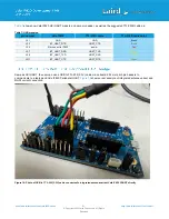
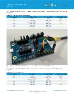
Page 22: ...CTS Brown No connect to IF820 power Red J1 20 P_UART_RXD HOST_TXD Orange J1 24 P_UART_TXD HOST_RXD Yellow J1 18 P_UART_CTS HOST_RTS Green Figure 19 Photo of USB to TTL 232 3 3V cable connected to MHF4...

Page 23: ...Please see the Vela IF820 series product page for links to the latest software documentation drawings schematics and more 1 Infineon CYW20820 DataSheet v01_00 EN 002 24743 Rev G Cypress Semiconductor...

Page 24: ...t pending Any information furnished by Laird Connectivity and its agents is believed to be accurate and reliable All specifications are subject to change without notice Responsibility for the use and...

Page 25: ...ird Connectivity and its agents cannot be aware of all potential uses Laird Connectivity makes no warranties as to non infringement nor as to the fitness merchantability or sustainability of any Laird...

Reviews: