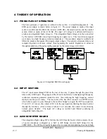
frequency current loops. In the half bridge ( 600w/ 1KW ) only one transistor is turned on at
a time. In the full bridge, the two diagonally opposite transistors Q1 and Q4 or Q2 and Q3
are turned on simultaneously. The result of this switching is to produce a quasi-square
waveform that is impressed on the primary of the power transformer. Each transistor is
protected by a fast recovery inverse parallel diode and by a turn-off snubbing network,
reducing the switching stress and associated power loss. Snubbing of voltage spikes induced
by the leakage inductance is implemented by R3 and C3 in the half bridge and by C7, R7A
and R7B in the full bridge. C17 and C18 in the full bridge and C4 and C5 in the half bridge
are used to ensure steady state Volt-Second balance across the primary of the power
transformer, this in turn prevents transformer saturation. The output of the A200 inverter
board is available at terminals HF1 and HF2.
4.4 OUTPUT SECTION
The high frequency power transformer T1 provides the necessary isolation and the step up or
step-down that is required for the output dc voltage. Fast recovery rectifiers (or Schottky
diodes for low voltage units) convert the secondary output into a unipolar pulse-width
waveform. Filtering is achieved with an LC combination.
4.5 A100 CONTROL BOARD
All of the control circuitry is located on the A100 Control Board. The board receives its
power from the bias transformer T2. The secondary of T2 is full-wave rectified and filtered.
The voltage regulators provide the regulated bias voltages ±15v (±12v for the 600W/1KW).
The bias voltages are used to power all the integrated circuits on the board. The control
circuitry includes the supervisory function, over current protection, Reference Generation,
Feedback and TRANSISTOR drive circuit.
4.5.1 SUPERVISORY FUNCTIONS
Most supervisory functions are performed by U4 and associated circuitry. These functions
include: Turn-on delay, Undervoltage lockout, Overvoltage protection, Mode detect, and
Remote Turn-on. In every fault condition Q5 is pulled low, activating the digital shutdown
ports on the PWM.
Turn-on Delay (soft-start)
U4 provides a three to four second delay by comparing the 5 Volt reference with the voltage
on C26. When power is applied, C26 charges through R34 with the necessary time constant
to provide the desired delay. During the delay (charging period of C26 to 5 volts), pin 1 of
U4 is negative turning off Q9 and thus disabling the relay K1. When the voltage across C26
reaches 5 volts, pin 1 of U4 goes positive turning on Q9, thereby activating the relay (K1)
which causes the bus charging resistor R1 to be shorted. At the same time, the CR17 clamp
on Q5 is released enabling the PWM.
Undervoltage Lockout
The unregulated side of the positive voltage regulator (an indirect measure of the AC input
voltage) is sensed through R17 and R18 at pin 6 of U4. When the unregulated voltage at
CR1 is below approx. 13V, pin 7 of U4 goes high, keeping Q5 fully on (saturated). Pin 5 &
8 of PWM (Pin 9 for the 600W/1KW) is thus clamped low by CR15 shutting down the
83-473-000 Revision J
4 - 2
Theory of Operation

