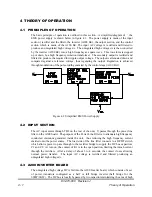
4.5.3 SET-POINT REFERENCE
Separate constant current sources provide reference voltages for the voltage and current
channels. The collector current of Q1 drives the
voltage control potentiometer
that is
located on the front panel, whereas Q2 drives the
current control potentiometer
. The
positive bias voltage supply is RC filtered with R8 and C10 to minimize noise feedthrough.
The current sources are referenced by the voltage across CR5, a temperature compensated
zener diode. The current from each of the sources is adjustable to 1mA by R3 and R5.
4.5.4 VOLTAGE CONTROL CHANNEL
Voltage control and error amplification are implemented by U6 and associated components.
The non-inverting input is routed from the (+) sensing terminal TB1/J1-2 (+V Rem) through
R49 and R50 attenuating the output voltage to a 0-5 volts level for 0-100% of the output
voltage. The inverting input is routed form TB1/J1-4 (V Amp In) through R51 and R53.
The signal at TB1/J1-4 is the voltage reference set by a 1mA current that flows through the
programming resistance R4 (in the normal mode of operation).
The voltage amplifier compares the reference and sense voltages and amplifies the error with
appropriate compensation for loop gain shaping. The R54, C40 feedback combination
provides a pole-zero combination, with a pole at DC for best DC regulation. The R51, C36,
R53 combination provides phase lead as required for overall loop stability. R55 is an offset
adjustment for zero nulling, and is set during calibration.
4.5.5 CURRENT CONTROL CHANNEL
Current control and error amplification are implemented by U5 (U8 for the 5KW) and
associated components. The non-inverting input is routed from the current shunt (+) sense
terminal TB1/J1-13 (Inv Amp In) through R45. The inverting input is routed from
TB1/J1-10 (I Amp In) through R44. The signal at TB1/J1-10 is the current reference set by
a 1mA current that flows through the programming resistance R5 (in the normal mode of
operation). The error amplifier U5 compares the reference and sense currents and amplifies the
error, with appropriate compensation provided by R44, R48, C29 and C31. Offset adjustment
is provided by R47 (R77 for the 5KW) and is set during calibration.
4.5.6 AUTOMATIC CROSSOVER
The outputs of the voltage and current channels are "ORed" via diodes CR31 and CR27, and
thus provide automatic crossover from current to voltage control, and vice versa. In the
600w/ 1KW and 2KW/2.5KW, the U5 and Q10 combination ensures that the current channel
output may never fall too far below the voltage output, thus reducing the transition time at
crossover. Additional attenuation of the analog channels' output is provided by R64, R65
and R66 (R67 and R68 for the 5KW) before the signal is fed to the input amplifier of the
modulator.
4.5.7 PULSE WIDTH MODULATOR FOR THE 600W/1KW
The PWM for the unit is a UC1524A IC. This IC performs several tasks. The main
function of the PWM is to convert the error signals from the voltage and current error
amplifiers to a pulse width modulated signal (CLK1 and CLK2) which is proportional to the
error voltage . The pulse width modulated signal is fed to the inverter to control the output
83-473-000 Revision J
4 - 4
Theory of Operation


