background image

AWARD BIOS SETUP 


AP-370VF/F / 38 


Video : 

Select the type of primary video subsystem in your computer.  The BIOS 

usually detects the correct video type automatically.    The BIOS supports a secondary 

video subsystem, but you do not select it in Setup. 

  EGA/VGA 

  Enhanced Graphics Adapter/Video Graphics Array.   

  For EGA, VGA, SEGA, SVGA or PGA monitor adapters. 

  CGA 40 

  Color Graphics Adapter, power up in 40 column mode 

  CGA 80 

  Color Graphics Adapter, power up in 80 column mode 

  MONO 

  Monochrome adapter, includes high resolution monochrome adapters 


Halt On : 

During the power-on-self-test (POST), the computer stops if the BIOS detects 

a hardware error.    You can tell the BIOS to ignore certain during the errors POST and 

continue the boot-up process.    These are the selections: 


  No errors 

  Whenever the BIOS detects a non-fatal error the system will not be 

  stopped and you will be prompted 

  All errors 

  The system boot will be stopped for any error that may be detected.   

  All, But Keyboard 

  The system boot will not stop for a keyboard error ; it will stop for all 

 Other errors. 

  All, But Diskette 

  The system boot will not stop for a disk error ; it will stop for all other   

 Errors. 

  All, But Disk/Key 

  The system boot will not stop for a keyboard or disk error ; it will stop   

  for all other errors. 

Summary of Contents for AP-370VF

Page 1: ...AP 370VF F Single Board Computer for Socket 370 Processors...

Page 2: ...ed by the purchaser for backup purposes All rights are reserved TRADEMARKS Pentium is a registered trademark of Intel Corporation The following are trademarks or registered trademarks of their respect...

Page 3: ...8 2 8 I O CONNECTOR SUMMARY FOR AP 370VF 19 2 9 SETTING STATUS INDICATORS AND CONTROL 20 CONNECTORS 2 10 I O CONNECTORS DESCRIPTION 21 CHAPTER 3 AWARD BIOS SETUP 32 3 1 RUNNING AWARD BIOS 32 3 2 CMOS...

Page 4: ...CHAPTER 4 DRIVERS SUPPORT 55 4 1 DRIVER DISKETTE LIST 55 4 2 AGP DRIVER UTILITIES 55 APPENDIX A HOW TO USE WATCH DOG TIMER 63 APPENDIX B TECHNICAL REFERENCE 64 GLOSSARY 66 TERMS AND CONDITIONS RMA SER...

Page 5: ...370VF is built as a PCI ISA expansion card that is simply upgraded by changing one card from another without replacing the whole system It provides the primary elements for building an IBM PC AT comp...

Page 6: ...support up to four Ultra DMA 33 IDE devices Floppy Drive Interface One FDD port up to two floppy devices Serial Port Two COM ports one RS 232 and one RS 232 422 485 serial port Parallel Port One mult...

Page 7: ...to 6 pin PS 2 AT keyboard connector EIDE Floppy cable 1 set 40 pin to 40 pin standard header flat ribbon cable 34 pin to 34 pin standard header flat ribbon cable Printer and COM ports cable 1 set 26...

Page 8: ...370VF 2 1 Board Outline of AP 370VF CHAPTER 2 COM1 VGA1 PKB1 PMS1 CPU RTC BATTERY JP2 1 3 10 12 DIO1 KCN1 COM2 JP13 1 2 9 10 JP10 1 3 JP11 JP9 JP8 JP7 6 PRT1 IR1 CON1 JP3 FDC1 FAN1 FAN2 JP1 JP14 JP12...

Page 9: ...allow experienced electronic technicians to do this job STATIC ELECTRICITY PRECAUTION Caution Computer components are very sensitive to damage from static electric discharge Always ground yourself to...

Page 10: ...ule must correspond with Pin1 of the socket 1 Pull the tabs which are at the ends of the socket to the side 2 Position the DIMM above the socket with the notches in the module aligned with the keys on...

Page 11: ...e jumper pins as designated by the required configuration as listed in this section A jumper is said to be on or 1 2 when the black cap has been placed on two of its pins as show in the figure below A...

Page 12: ...CONNECTORS AP 370VF F 8 2 4 JUMPER LOCATIONS FOR AP 370VF COM1 VGA1 PKB1 PMS1 CPU JP2 1 3 10 12 COM2 JP13 1 2 9 10 JP10 1 3 JP11 JP9 JP8 JP7 6 CON1 JP3 JP1 JP14 JP12 8 7 2 1 J1 11 20 AP 370VF1 1 JP4...

Page 13: ...JP1 Select CPU External Bus Clock JP2 Select Watch Dog Time Out Period JP3 Select Software Hardware Watch Dog JP4 JP5 Manufacturer Setting JP6 JP8 JP11 Select COM2 Type JP7 Select Clear CMOS Data JP1...

Page 14: ...PER SETTING AND CONNECTORS AP 370VF F 10 2 6 JUMPER SETTINGS FOR AP 370VF z JP1 Select CPU External Bus Clock JP1 Description ON 66MHz Default OFF 100MHz 1 JP1 2 66MHz 100MHz JP1 1 2 JP1 Default JP1 1...

Page 15: ...z JP2 Select Watch Dog Time Out Period Time Out Period JP4 0 5 sec 1 5 1 sec 2 6 2 sec 3 7 4 sec Default 4 8 16 sec 7 11 32 sec 6 10 64 sec 5 9 Default JP2 4 3 2 1 JP2 JP2 4 3 2 1 0 5 SEC 1 SEC 2 SEC...

Page 16: ...JUMPER SETTING AND CONNECTORS AP 370VF F 12 z JP3 Select Software Hardware Watch Dog JP3 Description ON Hardware Default OFF Software 1 JP3 2 Hardware Software JP3 1 2 JP3 Default JP3 1 2 JP3...

Page 17: ...8 JP9 JP10 JP11 RS 232 Default 1 2 1 2 RS 422 3 4 2 3 RS 485 5 6 2 3 Default JP8 JP9 JP10 JP11 JP6 JP8 JP10 3 1 3 3 JP11 JP9 3 1 1 1 JP6 3 1 2 6 4 5 RS 422 RS 485 RS 232 JP6 1 1 1 1 3 3 3 3 JP8 JP9 JP...

Page 18: ...lear CMOS OFF Default Normal Note To clear CMOS data turn power off and set JP7 ON Then turn power on and wait for 10 sec and CMOS data is cleared Be sure to power down the system and remove this jump...

Page 19: ...JP12 8 7 2 1 1 5X 2X Reserved JP12 z JP12 Select Internal CPU Clock Ratio Internal CPU Clock Ratio JP12 1 5 3 4 2 1 2 3 4 5 6 7 8 2 5 1 2 3 4 7 8 3 1 2 5 6 7 8 3 5 1 2 7 8 4 3 4 5 6 7 8 4 5 3 4 7 8 5...

Page 20: ...ation Address JP13 C800H C9FFH 1 2 7 8 D000H C1FFH 3 4 7 8 U33 D800H D9FFH 5 6 7 8 CC00H CDFFH 1 2 9 10 D400H D5FFH 3 4 9 10 U36 DC00H DDFFH 5 6 9 10 C800H C9FFH D000H D1FFH D800H D9FFH CC00H CDFFH JP...

Page 21: ...JUMPER SETTING AND CONNECTORS AP 370VF F 17 z JP14 On board AGP VGA Disable Enable JP14 On Board AGP ON Enable Default OFF Disable Default JP14 1 2 JP14 1 JP14 2 Enable Disable JP14 1 2 JP14...

Page 22: ...JUMPER SETTING AND CONNECTORS AP 370VF F 18 2 7 I O CONNECTOR LOCATIONS FOR AP 370VF COM1 VGA1 PKB1 PMS1 CPU DIO1 KCN1 COM2 PRT1 IR1 FDC1 FAN1 FAN2 IDE2 IDE1 USBC1 FAN3 AP 370VF 1 5 1 2 9 10...

Page 23: ...Fan1 Fan3 Fan Connector USBC1 USB Connector Pins KCN1 External Keyboard Connector Header COM1 COM1 Connector D Sub Connector COM2 COM2 Connector Header PKB1 PS2 Keyboard Connector 6 Pin Min DIN PMS1 P...

Page 24: ...L CONNECTORS CONNECTOR DESCRIPTION PIN NO DESCRIPTION 1 Power LED 2 Power LED Power LED 3 Power LED 4 Key Lock 1 Key Lock 5 Key Lock 2 7 VCC 8 NC 9 Buzzer Out Speaker 10 Speaker Signal 11 Reset Switch...

Page 25: ...D CONNECTORS AP 370VF F 21 2 10 I O CONNECTORS DESCRIPTION z DIO1 Digital Input Digital Output Ports Header PIN NO DESCRIPTION 1 IN0 2 OUT0 3 IN1 4 OUT1 5 IN2 6 OUT2 7 IN3 8 OUT3 9 Ground 10 Ground 1...

Page 26: ...JUMPER SETTING AND CONNECTORS AP 370VF F 22 z FAN1 Fan Connector PIN NO DESCRIPTION 1 Ground 2 12V 3 FAN Status z FAN2 Fan Connector PIN NO DESCRIPTION 1 Ground 2 12V 3 NC FAN1 1 3 FAN1 FAN2 FAN2 1 3...

Page 27: ...DESCRIPTION 1 Ground 2 12V 3 FAN Status z USBC1 USB Connector PIN NO DESCRIPTION 1 USB Port 0 VCC 2 USB Port 0 D0 3 USB Port 0 D0 4 Ground 5 USB Port 1 Ground 6 USB Port 1 VCC 7 USB Port 1 D1 8 USB Po...

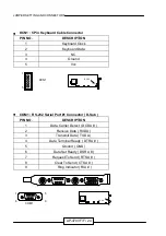
Page 28: ...yboard Data 3 NC 4 Ground 5 Vcc z COM1 RS 232 Serial Port 1 Connector D Sub PIN NO DESCRIPTION 1 Data Carrier Detect DCDA 2 Receive Data RXDA 3 Transmit Data TXDA 4 Data Terminal Ready DTRA 5 Ground G...

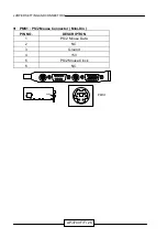
Page 29: ...O RS 232 RS 422 RS 485 1 DCDB TX DATA 2 RXDB TX DATA 3 TXDB RX NC 4 DTRB RX NC 5 Ground Ground Ground 6 DSRB NC NC 7 RTSB NC NC 8 CTSB NC NC 9 RIB NC NC 10 NC NC NC z PKB1 PS 2 Keyboard Connector Mini...

Page 30: ...JUMPER SETTING AND CONNECTORS AP 370VF F 26 z PMS1 PS 2 Mouse Connector Mini Din PIN NO DESCRIPTION 1 PS 2 Mouse Data 2 NC 3 Ground 4 5V 5 PS 2 Mouse Clock 6 NC PMS1 PMS1...

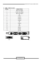
Page 31: ...370VF F 27 z VGA1 VGA Connector PIN NO DESCRIPTION 1 Red Color Signal 2 Green Color Signal 3 Blue Color Signal 4 NC 5 Ground 6 Ground 7 Ground 8 Ground 9 NC 10 Ground 11 NC 12 SPD 13 H Sync 14 V Sync...

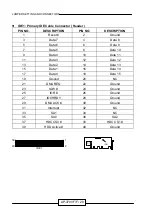
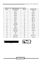
Page 32: ...ata 6 6 Data 9 7 Data 5 8 Data 10 9 Data 4 10 Data 11 11 Data 3 12 Data 12 13 Data 2 14 Data 13 15 Data 1 16 Data 14 17 Data 0 18 Data 15 19 Ground 20 NC 21 DMA REQ 22 Ground 23 IOW 24 Ground 25 IOR 2...

Page 33: ...Data 6 6 Data 9 7 Data 5 8 Data 10 9 Data 4 10 Data 11 11 Data 3 12 Data 12 13 Data 2 14 Data 13 15 Data 1 16 Data 14 17 Data 0 18 Data 15 19 Ground 20 NC 21 DMA REQ 22 Ground 23 IOW 24 Ground 25 IOR...

Page 34: ...und 6 DS1 7 Ground 8 Index 9 Ground 10 Motor Enable A 11 Ground 12 Drive Select B 13 Ground 14 Drive Select A 15 Ground 16 Motor Enable B 17 Ground 18 Direction 19 Ground 20 Step 21 Ground 22 Write Da...

Page 35: ...PTION 1 Strobe 2 Auto Form Feed 3 Data 0 4 Error 5 Data 1 6 Initialize 7 Data 2 8 Printer Select IN 9 Data 3 10 Ground 11 Data 4 12 Ground 13 Data 5 14 Ground 15 Data 6 16 Ground 17 Data 7 18 Ground 1...

Page 36: ...e POST routines perform various diagnostic checks while initializing the board hardware If the routines encounter an error during the tests the error will be reported in either of two ways a series of...

Page 37: ...SETUP DEFAULTS INTEGRATED PERIPHERALS SUPERVISOR PASSWORD USER PASSWORD IDE HDD AUTO DETECTION HDD LOW LEVEL FORMAT SAVE EXIT SETUP EXIT WITHOUT SAVING ESC Quit Select Item F10 Save Exit Setup Shift F...

Page 38: ...Drive B 1 44M 3 5 in None Base Memory Extended Memory Other Memory 640K 195584K 384K Video Halt On EGA VGA All But Keyboard Total Memory 196608K ESC Quit Select Item PU PD Modify F1 Help Shift F2 Chan...

Page 39: ...ogram screen to enter the drive specifications Here is a brief explanation of drive specifications z Type The BIOS contains a table of pre defined drive types Each defined drive type has specified num...

Page 40: ...AWARD BIOS SETUP AP 370VF F 36 The AWARD BIOS supports three HDD modes NORMAL LBA and LARGE...

Page 41: ...reverse transformation process will be made inside INT13H in order to access to the right HDD address The maximum HDD size that is supported by the LARGE mode is 1 Gigabytes Note 1 To support LBA or...

Page 42: ...rs Halt On During the power on self test POST the computer stops if the BIOS detects a hardware error You can tell the BIOS to ignore certain during the errors POST and continue the boot up process Th...

Page 43: ...y Drive Disabled Boot Up Floppy Seek Disabled Boot Up NumLock Status On Gate A20 Option Fast Typematic Rate Setting Disabled Typematic Rate Chars Sec 6 Typematic Delay M Sec 250 Security Option Setup...

Page 44: ...CDROM A This setting determines where the computer looks first for an operating system the hard disk or the floppy disk or other The BIOS will load the operating system from the disk drives in the seq...

Page 45: ...port and you install a serial pointing device select Disabled PCI VGA Palette Snoop The default setting is Disabled Set to Enable if any ISA adapter card installed requires VGA palette snooping Assig...

Page 46: ...me 3 Current CPUFAN1 Speed 0RPM SDRAM Precharge Control Disabled Current CPUFAN2 Speed 0RPM DRAM Data Integrity Mode Non ECC Vcore 1 96V 3 3V 3 23V System BIOS Cacheable Enabled 5V 4 96V 12V 12 22V Vi...

Page 47: ...synchronous DRAM is installed in the system SDRAM RAS Precharge Time If an insufficient number of cycles is allowed for the RAS to accumulate its charge before DRAM refresh the refresh may be incompl...

Page 48: ...ed to PCI or ISA Thus there will be a 1M Bytes hole in your system memory This option is designed for some OS with special add on cards which need 15M 16M memory space Passive Release The default sett...

Page 49: ...d into your system will be activated Current System Temp The temperature of the system is 37o C 98o F This field displays the current system temperature if your computer contains a monitoring system C...

Page 50: ...abled Doze Mode Disabled Secondary IDE 1 Disabled Standby Mode Disabled Floppy Disk Disabled Suspend Mode Disabled Serial Port Enabled HDD Power Down Disabled Parallel Port Disabled Throttle Duty Cycl...

Page 51: ...Activity of the selected IRQ always awakens the system The default setting is 3 Doze Mode Options are from 1 Min to 1 Hour and Disable The system speed will change from turbo to slow and the video sig...

Page 52: ...rial Ring Indicator RI line awakens the system from soft off state IRQ8 Clock Event You can turn On or Off monitoring of IRQ8 the Real Time Clock so it does not awaken the system from Suspend mode Rel...

Page 53: ...uration Data Disabled Assign IRQ For USB Enabled IRQ 3 assigned to Legacy ISA IRQ 4 assigned to Legacy ISA IRQ 5 assigned to PCI ISA PnP IRQ 7 assigned to Legacy ISA IRQ 9 assigned to PCI ISA PnP IRQ...

Page 54: ...use BIOSes fail to auto detect some specific ISA Legacy cards with requested memory space below 1M address we have added the Used MEM base addr and Used MEM Length to support such kind of cards Now wi...

Page 55: ...S SETUP CHIPSET FEATURES SETUP POWER MANAGEMENT SETUP PNP PCI CONFIGURATION LOAD BIOS DEFAULTS LOAD SETUP DEFAULTS INTEGRATED PERIPHERALS SUPERVISOR PASSWORD USER PASSWORD IDE HDD AUTO DETECTION HDD L...

Page 56: ...DRIVERS SUPPORTARD BIOS SETUP AP 370VF F 52 proceed...

Page 57: ...lave UMDA Auto IDE Secondary Master UMDA Auto IDE Secondary Slave UMDA Auto On Chip Primary PCI IDE Enabled On Chip Secondary PCI IDE Enabled USB Keyboard Support Disabled Init display First PCI Slot...

Page 58: ...PCI IDE The default setting is Enabled This option enables the onboard Primary Secondary PCI IDE controller USB Keyboard Support Select Enabled if your system contains a Universal Serial Bus USB contr...

Page 59: ...R PASSWORD The SUPERVISOR USER PASSWORD utility sets the password The SBC is shipped with the password disabled If you want to change the password you must first enter the current password then at the...

Page 60: ...rts LBA mode more than one line will appear in the parameter box choose the line that lists LBA for an LBA drive Do not choose Large or Normal if the hard disk drive is already fully formatted when yo...

Page 61: ...Diskette No Driver Directory Name CD ROM No 1 Genisys Vga 4 2 AGP DRIVER UTILITIES This section describes the operation and installation of the software drivers Below is the Windows 95 98 Driver Insta...

Page 62: ...VERS SUPPORT AP 370VF F 58 Step 2 In the Control Panel window select the Display icon and double click to proceed to the configuration Step 3 In the Display Properties window click on the Settings fol...

Page 63: ...RT AP 370VF F 59 Step 4 In the Display Properties window select the Settings folder and click on the Advanced Properties tab to continue Step 5 In the Advanced Display Properties click Change under Ad...

Page 64: ...DRIVERS SUPPORT AP 370VF F 60 Step 6 When the Select Device window appears select and click Have Disk tab Step 7 Under the Install From Disk window select Browse tab and click to continue...

Page 65: ...n window appear as shown below Move tab in the dialog box of Drives A pull out box showing the available drives Select and point to d and click to start reading d drive Step 9 In the Open window selec...

Page 66: ...DRIVERS SUPPORT AP 370VF F 62 Step 10 Select vga file in the Folders d ap 370vf open filed Step 11 Select win9x file in the Folders d ap 370vf vga open filed...

Page 67: ...F 63 Step 12 The Open window appears select utility driver Step 13 Select and point to s3lc2x inf under the File name dialog box Click OK to proceed Step 14 When the Install From Disk window appears...

Page 68: ...the Select Device window click OK tab to start installation Step 16 The driver program will be retrieved and install in the system Step 17 The System Settings Change window appears select Yes tab and...

Page 69: ...refer to the chapter on jumper settings and connectors During the period of enable to reset you could still cancel reset by disabling the watch dog EX 1 For DOS Execute the DEBUG EXE file under DOS Th...

Page 70: ...r 2 0C0 0DF DMA Controller 2 0F0 0F1 Clear Reset Math Coprocessor 1F0 1F7 Hard Disk Controller 200 210 Game Port 278 27F Parallel Port 2 2E8 2EF Serial Port 4 COM 4 2F8 2FF Serial Port 2 COM 2 300 31F...

Page 71: ...Disk Controller DMA 3 ECP Parallel Port DMA 4 Cascade for DMA 1 DMA 5 Reserved DMA 6 Reserved DMA 7 Reserved INTERRUPT CONTROLLER IRQ Function IRQ 0 System timer output IRQ 1 Keyboard IRQ 2 Cascade f...

Page 72: ...a repeater Adapter It is also called an expansion board expansion card or adapter card It is a small circuit board that is installed in the expansion slots on the motherboard You can install a partic...

Page 73: ...sk or even RAM so a cache helps the system work more efficiently Most systems sold today offer either 256K or 512K cache CPU Central Processing Unit executes all commands and controls the flow of data...

Page 74: ...rity checking improvements over SCSI 1 IDE Integrated Drive Electronics It was developed from ST 506 type hard drive interface utilizes BIOS INT 13h hard drive secondary software and supports two hard...

Page 75: ...h PC a thorough check up Additionally this feature is available to multiple OS s on the market today LDCM Key Features include the following Health Monitoring Real Time Alerting Remote Accessibility E...

Page 76: ...it s your first warning of trouble with any of the components When the POST detects an error from the display memory keyboard or other basic components it produces an error warning in the form of a m...

Page 77: ...I 3 is a third generation SCSI standard that introduced parallel bus speed improvements FAST 20 and FAST 40 an the miniaturized 68 pin micro connector USB Universal Serial Bus USB consolidates serial...

Page 78: ...will be returned at the customer expense 5 The following conditions are excluded from this warranty A Improper or inadequate maintenance by the customer B Unauthorized modification or misuse C Operat...

Page 79: ...Return Shipping Address For Supplier only RMA No Account Sales Model No Serial No Problem Code Remark This form could be copied for more description Problem Code 01 D O A 02 Second Time R M A 03 No Sc...

Reviews: