background image

JUMPER SETTING AND CONNECTORS 


AP-545L/27 

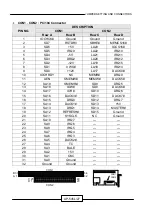
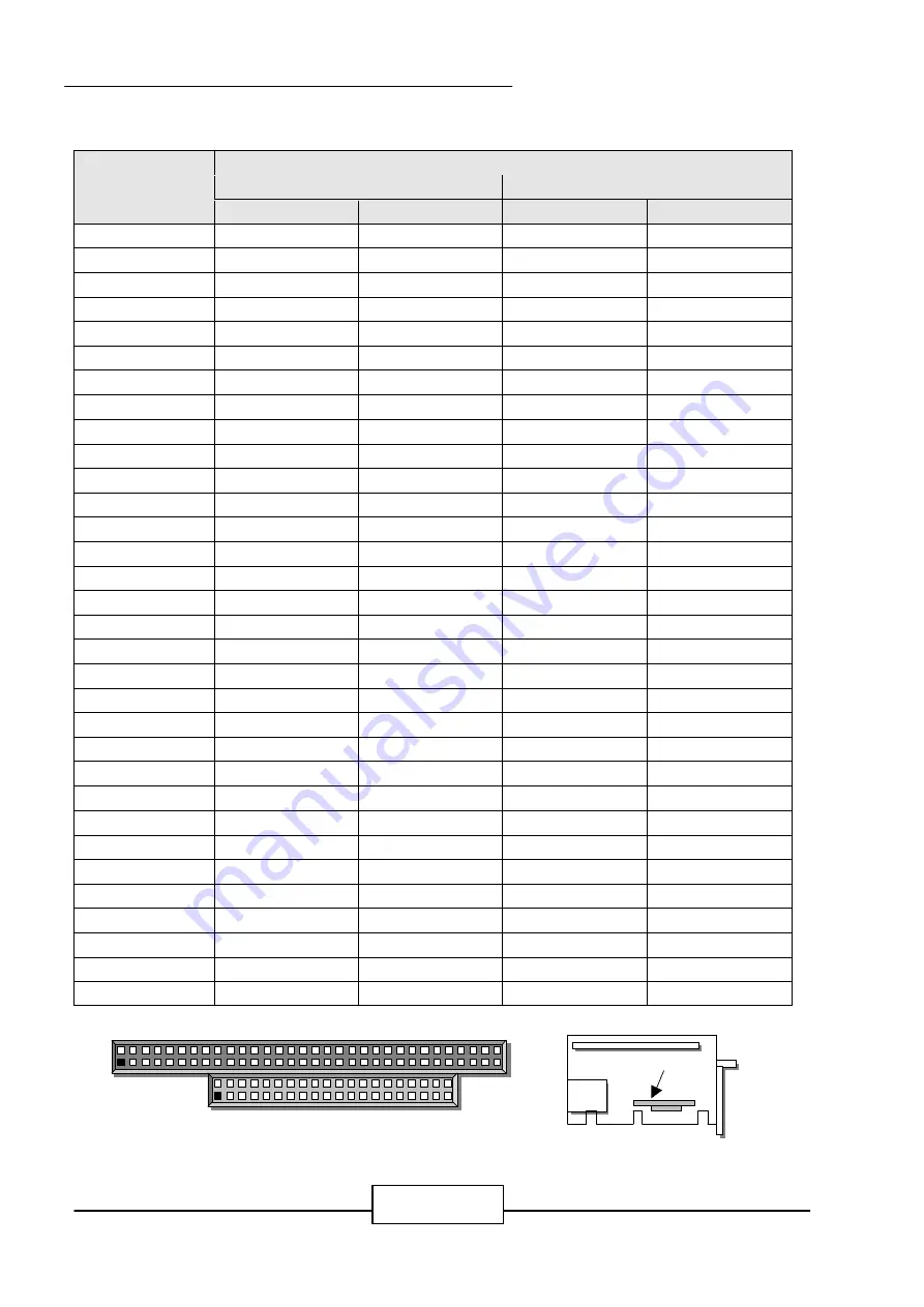
CON1 , CON2 : PC/104 Connector 

DESCRIPTION 

CON1 

CON2 


PIN NO. 

Row A 

Row B 

Row C 

Row D 

IOCHCK# 

Ground 

Ground 

Ground 

SD7 

RSTDRV 

SBHE# 

MEMCS16# 

SD6 

+5V 

LA23 

IOCS16# 

SD5 

IRQ9 

LA22 

IRQ10 

SD4 

-5V 

LA21 

IRQ11 

SD3 

DRQ2 

LA20 

IRQ12 

SD2 

-12V 

LA19 

IRQ15 

SD1 

0 WS# 

LA18 

IRQ14 

SD0 

+12V 

LA17 

DACK0# 

10 

IOCHRDY 

NC 

MEMR# 

DRQ0 

11 

AEN 

SMEMW# 

MEMW# 

DACK5# 

12 

SA19 

SMEMR# 

SD8 

DRQ5 

13 

SA18 

IOW# 

SD9 

DACK6# 

14 

SA17 

IOR# 

SD10 

DRQ6 

15 

SA16 

DACK3# 

SD11 

DACK7# 

16 

SA15 

DRQ3 

SD12 

DRQ7 

17 

SA14 

DACK1# 

SD13 

+5V 

18 

SA13 

DRQ1 

SD14 

MASTER# 

19 

SA12 

REFRESH# 

SD15 

Ground 

20 

SA11 

SYSCLK 

NC 

Ground 

21 

SA10 

IRQ7 

--- 

--- 

22 

SA9 

IRQ6 

--- 

--- 

23 

SA8 

IRQ5 

--- 

--- 

24 

SA7 

IRQ4 

--- 

--- 

25 

SA6 

IRQ3 

--- 

--- 

26 

SA5 

DACK2# 

--- 

--- 

27 

SA4 

TC 

--- 

--- 

28 

SA3 

BALE 

--- 

--- 

29 

SA2 

+5V 

--- 

--- 

30 

SA1 

OSC 

--- 

--- 

31 

SA0 

Ground 

--- 

--- 

32 

Ground 

Ground 

--- 

--- 


32


64


CON1


B


A


C


CON2


20


D


1


21


33


1


40


CON1 
CON2 

Summary of Contents for AP-545L

Page 1: ...AP 545L Single Board Computer with VGA LCD for ZIF Socket 7 Processor The contents information in this manual are subject to change without prior notice For reference only ...

Page 2: ... the purchaser for backup purposes All rights are reserved TRADEMARKS Pentiumâ is a registered trademark of Intel Corporation The following are trademarks or registered trademarks of their respective companies IBM Intel AMD Cyrix Award AMI Microsoft Windows Windows NT Novell SCO PC 104 PICMG ALI UMC SMC Winbond Products mentioned in this manual are mentioned for identification purposes only All na...

Page 3: ... FOR AP 545L 8 2 7 I O CONNECTORS LOCATION FOR AP 545L 14 2 8 I O CONNECTORS SUMMARY FOR AP 545L 15 2 9 SETTING STATUS INDICATORS AND CONTROL 16 CONNECTORS 2 10 I O CONNECTORS DESCRIPTION 17 CHAPTER 3 AMI BIOS SETUP 28 3 1 RUNNING AMI BIOS 28 3 2 AMI BIOS HIFLEX SETUP UTILITY 29 3 3 STANDARD CMOS SETUP 30 3 4 ADVANCED CMOS SETUP 34 3 5 ADVANCED CHIPSET SETUP 39 3 6 POWER MANAGEMENT SETUP 41 3 7 PC...

Page 4: ......

Page 5: ...TABLE OF CONTENTS APPENDIX A HOW TO USE WATCH DOG TIMER 53 APPENDIX B TECHNICAL REFERENCE 54 APPENDIX C PC 104 MODULE INSTALLATION 56 GLOSSARY 57 TERMS AND CONDITIONS RMA SERVICE REQUEST FORM ...

Page 6: ......

Page 7: ... IBM PC AT compatible computer for a wide variety of applications with system integration The AP 545L is fully compatible with the IBM PC AT which means virtually all the software written for the IBM PC AT will run on the AP 545L SBC Other on board features include two serial ports one each of RS 232 and RS 232 422 485 one multi mode parallel ECP EPP SPP port a floppy drive controller and a keyboa...

Page 8: ...E devices and Ultra DMA 33 o Floppy Drive Interface One FDD port support up to two floppy devices o Serial Port Two COM ports one RS 232 and one RS 232 422 485 serial ports o Parallel Port One multi mode parallel port SPP EPP ECP o Bus Interface ISA bus o RTC Battery Dallas RTC battery or compatible o DMA 8 DMA channels o Interrupts 16 levels of hardware interrupts o PS 2 Mouse Keyboard On board 6...

Page 9: ... Mouse adapter cable 1 set 6 pin PS 2 to 5 pin PS 2 keyboard mouse connector IDE Floppy cable 1 pc 40 pin standard header to 40 pin standard header 34 pin standard header to 34 pin standard header Printer COM port cable 1 set 26 pin female flat connector t header to 25 pin female D Sub connector 10 pin standard flat header to 9 pin D Sub cable LCD VGA Utility Drivers 1 pc CD ROM diskette User s ma...

Page 10: ...ocation on the AP 545L CHAPTER 2 PKM1 DIMM1 AP 545L 3 JP2 SiS 5582 l BZ1 JP10JP11 JP13 JP12 JP9 IDE1 COM2 1 5 JP5 KCN1 8 J5 J4 15 1 1 2 3 J3 1 CON1 CON2 JP4 1 1 3 8 1 2 7 1 2 5 6 J1 JP7 1 3 J2 CN2 JP6 FAN1 2 7 8 JP1 1 3 VGA1 COM1 Socket 7 1 1 1 1 SMI 811 l RTC BATTERY 6 2 2 7 8 USBC1 1 1 PS1 16 JP8 JP3 1 2 5 6 FDC1 PRT1 ...
Page 11: ...the boards in the computer Use a grounding wrist strap at all time Place all electronic components on the anti static pad for static dissipation or in a static shielded bag when they are not in the chassis 2 3JUMPER SETTING OVERVIEW In order to select the operation modes of your system configure and set the jumpers on the your SBC to match the need of your application To set a jumper a black plast...

Page 12: ...UMPER SETTING AND CONNECTORS AP 545L 6 2 4 JUMPER LOCATION FOR AP 545L AP 545L JP10JP11 JP13 JP12 JP9 1 5 JP5 8 15 1 2 J3 1 JP4 1 3 2 7 1 2 5 6 JP7 1 3 JP6 2 7 8 JP1 1 Socket 7 1 1 1 1 6 2 16 JP3 1 2 5 6 ...

Page 13: ...MARY FOR AP 545L JUMPERS LOCATION FUNCTION JP1 Select CPU Vcore Voltage JP3 Select CPU External Bus Clock JP4 Select Internal CPU Clock Ratio JP5 Select Disk On Chip Flash Disk Address JP6 JP7 Select ISP GAL Function JP9 JP13 Select COM2 Type J3 Select Panel Type ...

Page 14: ...1 2 3 4 2 4 V 5 6 2 5 V 1 2 5 6 2 6 V 3 4 5 6 2 7 V 1 2 3 4 5 6 2 8 V Default 7 8 2 9 V 1 2 7 8 3 0 V 3 4 7 8 3 1 V 1 2 3 4 7 8 3 2 V 5 6 7 8 3 3 V 1 2 5 6 7 8 3 4 V 3 4 5 6 7 8 3 5 V 1 2 3 4 5 6 7 8 Default 1 3 5 7 JP1 2 4 6 8 JP1 2 4 6 8 JP1 1 3 5 7 2 0V 2 1V 2 2V 2 3V 2 4V 2 5V 2 6V 2 7V 2 8V 2 9V 3 0V 3 1V 3 2V 3 3V 3 4V 3 5V 1 3 5 7 JP1 2 4 6 8 JP1 ...

Page 15: ...ng 50 60 66 6 60 66 6 60 66 6 66 6 66 6 Frequency ratio 1 5 1 5 1 5 2 2 2 5 2 5 3 3 5 l JP3 Select CPU External Bus Clock Phase Link PLL52C66 01 CPU External Bus Clock JP3 50 MHz 1 2 3 4 5 6 60 MHz 1 2 66 6 MHz Default OFF 75 MHz 3 4 5 6 JP3 Default JP3 2 4 6 1 3 5 50MHz 60MHz 66 6MHz 75MHz JP3 JP3 5 2 6 1 4 3 1 3 5 JP3 2 4 6 ...

Page 16: ...al CPU Clock Ratio Clock Ratio JP4 1 5 X OFF 2 0 X 1 2 2 5 X Default 1 2 3 4 3 0 X 3 4 3 5 X OFF 4 0 X 1 2 5 6 4 5 X 1 2 3 4 5 6 5 0 X 3 4 5 6 5 5 X 5 6 Default 1 3 5 JP4 2 4 6 JP4 1 3 5 JP4 2 4 6 1 3 5 JP4 2 4 6 1 5X 2 0X 2 5X 3 0X 4 0X 4 5X 5 0X 5 5X 3 5X JP4 ...

Page 17: ... 4 7 8 Note Spare Jumper at 2 4 6 8 l P6 JP7 Select ISP GAL Function ISP GAL Function JP6 JP7 Program ISP GAL 2 3 2 3 Use Watch Dog Default 1 2 1 2 Default JP5 JP5 8 2 1 5 4 6 3 7 Default 1 JP6 3 2 1 2 3 JP7 JP6 JP7 JP6 JP7 Program ISP GAL 1 JP6 3 2 1 2 3 JP7 Use Watch Dog 1 3 JP6 2 3 1 2 JP7 D0000 D1FFFH D4000 D5FFFH D8000 D9FFFH DC000 DDFFFH JP5 8 2 1 5 4 6 3 7 6 5 JP5 1 2 3 7 4 JP5 ...

Page 18: ...11 JP12 JP13 RS 232 Default 1 2 1 2 1 2 1 2 1 2 RS 422 3 4 2 3 2 3 2 3 2 3 RS 485 5 6 2 3 2 3 2 3 2 3 Default JP9 2 JP12 JP13 JP10 JP11 6 1 5 1 1 1 1 3 3 3 3 JP9 JP10 JP13 RS 232 RS 422 RS 485 JP9 JP10 JP13 JP9 2 JP12 JP13 JP10 JP11 6 1 5 1 1 1 1 3 3 3 3 JP13 6 5 JP9 JP11 JP10 JP12 1 2 1 2 3 ...

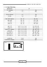
Page 19: ... ON OFF 1280 x 1K 5 6 7 8 OFF OFF 9 BIT TFT 9 10 11 12 13 14 ON ON ON 12 BIT TFT 9 10 11 12 13 14 OFF ON ON 18 BIT TFT Default 9 10 11 12 13 14 ON OFF ON 24 BIT TFT 9 10 11 12 13 14 OFF OFF ON 12 x 2 BIT TFT 9 10 11 12 13 14 ON ON OFF ANALOG TFT 9 10 11 12 13 14 OFF ON OFF 18 x 2 BIT TFT 9 10 11 12 13 14 ON OFF OFF 16 BIT STN 15 16 ON 24 BIT STN Default 15 16 OFF Default J3 2 J3 6 1 4 15 8 3 5 7 9...

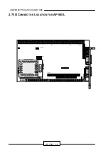
Page 20: ...JUMPER SETTING AND CONNECTORS AP 545L 14 2 7I O CONNECTOR LOCATION FOR AP 545L PKM1 AP 545L IDE1 COM2 KCN1 J5 J4 1 3 CON1 CON2 1 8 1 J1 J2 CN2 FAN1 3 VGA1 COM1 Socket 7 2 7 8 USBC1 1 PS1 FDC1 PRT1 CN1 1 ...
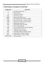
Page 21: ...e Connector Header COM1 RS 232 Serial Part 1 Connector D Sub COM2 RS 232 Serial Part 2 Connector Header PS1 External Power Connector VGA1 VGA Monitor Connector D Sub J4 VGA Connector Header PKM1 PS 2 Keyboard Mouse Connector Mini Din CN1 Program ISP GAL Connector CN2 LCD Panel Connector Header IDE1 Primary IDE Interface Connector Header FDC1 Floppy Interface Connector Header PRT1 Parallel Interfac...

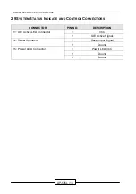
Page 22: ...16 2 9SYSTEM STATUS INDICATE AND CONTROL CONNECTORS CONNECTOR PIN NO DESCRIPTION J1 IDE Active LED Connector 1 VCC 2 IDE Active Signal J2 Reset Connector 1 Reset Input Signal 2 Ground J5 Power LED Connector 1 Power LED VCC 2 Ground 3 Ground ...

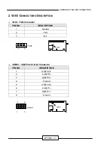
Page 23: ...0 I O CONNECTORS DESCRIPTION l FAN1 FAN Connector PIN NO DESCRIPTION 1 Ground 2 12V 3 NC l USBC1 USB Port 1 2 Connector PIN NO DESCRIPTION 1 USB VCC 2 USB P0 3 USB P0 4 Ground 5 USB VCC 6 USB P1 7 USB P1 8 Ground FAN1 1 3 FAN1 USBC1 USBC1 7 8 2 1 ...

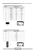
Page 24: ...oard Data 3 Ext Power Good 4 Ground 5 5V l COM1 RS 232 Serial Port 1 Connector D Sub PIN NO DESCRIPTION 1 Data Carrier Detect DCDA 2 Receive Data RXDA 3 Transmit Data TXDA 4 Data Terminal Ready DTRA 5 Ground GND 6 Data Set Ready DSRA 7 Request To Send RTSA 8 Clear To Send CTSA 9 Ring Indicator RIA 1 5 KCN1 KCN1 COM1 COM1 5 9 6 1 ...

Page 25: ...NO RS 232 RS 422 RS 485 1 DCDB TX DATA 2 RXDB TX DATA 3 TXDB RX NC 4 DTRB RX NC 5 Ground Ground Ground 6 DSRB NC NC 7 RTSB NC NC 8 CTSB NC NC 9 RIB NC NC 10 NC NC NC l PS1 External Power Connector Header PIN NO DESCRIPTION 1 5V 2 12V 3 12V 4 Ground 5 Ground 6 5V 7 12V 8 5V 10 5 6 1 COM2 COM2 PS1 1 8 PS1 ...

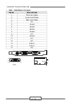
Page 26: ...545L 20 l VGA1 VGA Monitor Connector PIN NO DESCRIPTION 1 Red Color Signal 2 Green Color Signal 3 Blue Color Signal 4 NC 5 Ground 6 Ground 7 Ground 8 Ground 9 NC 10 Ground 11 NC 12 NC 13 H Sync 14 V Sync 15 NC VGA1 VGA1 5 1 6 10 11 15 ...

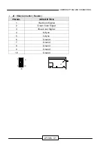
Page 27: ...ING AND CONNECTORS AP 545L 21 l J4 VGA Connector Header PIN NO DESCRIPTION 1 Red Color Signal 2 Green Color Signal 3 Blue Color Signal 4 H Sync 5 V Sync 6 Ground 7 Ground 8 Ground 9 Ground 10 Ground 10 1 6 5 J4 J4 ...

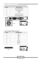
Page 28: ...ouse Connector Mini Din PIN NO DESCRIPTION 1 PS 2 Keyboard Data 2 PS 2 Mouse Data 3 Ground 4 VCC 5 PS 2 Keyboard Clock 6 PS 2 Keyboard Clock l CN1 Program ISP GAL Connector PIN NO DESCRIPTION 1 VCC 2 SDO 3 SDI 4 ISP 5 NC 6 MODE 7 Ground 8 SCLK PKM1 PKM1 CN1 8 1 CN1 ...

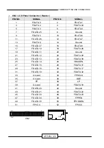
Page 29: ...4 Ground 15 FDATA 27 16 FDATA 9 17 FDATA 10 18 FDATA 28 19 FDATA 11 20 Ground 21 FDATA 12 22 FDATA 29 23 FDATA 13 24 FDATA 30 25 FDATA 14 26 VBIASEN 27 FDATA 15 28 FDATA 31 29 FDATA 16 30 FDATA 17 31 FDATA 18 32 FDATA 32 33 Ground 34 FPSCLK 35 Ground 36 DDE 37 FP 38 LP 39 Ground 40 FDATA 19 41 FDATA 20 42 Ground 43 FDATA 21 44 FDATA 22 45 FDATA 33 46 FDATA 23 47 FDATA 34 48 FPPEN 49 FDATA 35 50 FP...

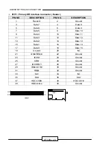
Page 30: ... Data 6 6 Data 9 7 Data 5 8 Data 10 9 Data 4 10 Data 11 11 Data 3 12 Data 12 13 Data 2 14 Data 13 15 Data 1 16 Data 14 17 Data 0 18 Data 15 19 Ground 20 NC 21 DMA REQ 22 Ground 23 IOW 24 Ground 25 IOR 26 Ground 27 IOCHRDY 28 Ground 29 DMA ACK 30 Ground 31 IRQ 32 Ground 33 SA1 34 NC 35 SA0 36 SA2 37 HDC CS0 38 HDC CS1 39 HDD Active 40 Ground IDE1 39 40 2 1 IDE1 ...

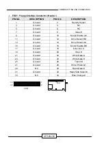
Page 31: ...round 6 NC 7 Ground 8 Index 9 Ground 10 Motor Enable A 11 Ground 12 Drive Select B 13 Ground 14 Drive Select A 15 Ground 16 Motor Enable B 17 Ground 18 Direction 19 Ground 20 Step 21 Ground 22 Write Data 23 Ground 24 Write Gate 25 Ground 26 Track 0 27 Ground 28 Write Protect 29 NC 30 Read Data 31 Ground 32 Head Side Select 33 NC 34 Disk Change FDC1 2 1 33 34 FDC1 ...

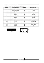
Page 32: ...CRIPTION 1 Strobe 14 Ground 2 Auto Form Feed 15 Data 6 3 Data 0 16 Ground 4 Error 17 Data 7 5 Data 1 18 Ground 6 Initialize 19 Acknowledge 7 Data 2 20 Ground 8 Printer Select IN 21 Busy 9 Data 3 22 Ground 10 Ground 23 Paper Empty 11 Data 4 24 Ground 12 Ground 25 Printer Select 13 Data 5 26 NC PRT1 14 1 13 26 PRT1 ...

Page 33: ...WS LA18 IRQ14 9 SD0 12V LA17 DACK0 10 IOCHRDY NC MEMR DRQ0 11 AEN SMEMW MEMW DACK5 12 SA19 SMEMR SD8 DRQ5 13 SA18 IOW SD9 DACK6 14 SA17 IOR SD10 DRQ6 15 SA16 DACK3 SD11 DACK7 16 SA15 DRQ3 SD12 DRQ7 17 SA14 DACK1 SD13 5V 18 SA13 DRQ1 SD14 MASTER 19 SA12 REFRESH SD15 Ground 20 SA11 SYSCLK NC Ground 21 SA10 IRQ7 22 SA9 IRQ6 23 SA8 IRQ5 24 SA7 IRQ4 25 SA6 IRQ3 26 SA5 DACK2 27 SA4 TC 28 SA3 BALE 29 SA2...

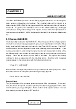
Page 34: ... routines perform various diagnostic checks while initializing the board hardware If the routines encounter an error during the tests the error will be reported in either of the two different ways hear a series of short beeps or see an error message on the screen display There are two kinds of error fatal or non fatal The system can usually continue to boot up sequence with the non fatal errors No...

Page 35: ...e User Password Change Supervisor Password Change Language Setting Auto Configuration with Optimal Settings Auto Configuration with Fail Safe Settings Save Settings and Exit Exit Without Saving Standard CMOS setup for changing time date hard disk type etc ESC Exit Sel F2 F3 Color F10 Save Exit This screen provides access to the utility s various functions Listed below are the explanation of the ke...

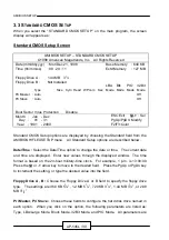
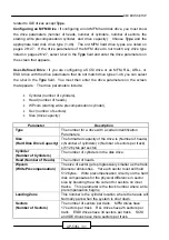
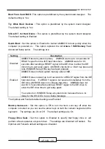
Page 36: ...e Standard field from the AMIBIOS HIFLEX SETUP menu All Standard Setup options are described below Date Time Select the Date Time option to change the date or time The current date and time are displayed Enter new values through the displayed window The time format is based on the 24 hour military time clock For example 1 p m is 13 00 00 Press the or arrow key to move to the desired field Press th...

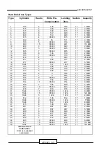
Page 37: ...ompensation cylinder l Sec number of sectors l Size drive capacity Parameter Description Type The number for a drive with a certain identification Parameters Size Hard Disk Drive Capacity The formatted capacity of the drive is Number of heads x Number of cylinders x Number of sectors per track x 512 bytes per sector Cylinder Number of Cylinders The number of cylinders in the disk drive Head Number...

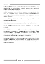
Page 38: ...B Click on Block Mode and choose On to support IDE drives that use Block Mode Click on 32Bit Mode and click on On to support for IDE drive that permit 32 bit accesses Click on PIO Mode to select the IDE Programmed I O mode PIO programming also works with ATAPI CD ROM drives The settings are Auto 0 1 2 3 4 or 5 Click on Auto to allow AMIBIOS to automatically find the PIO mode that the IDE drive bei...

Page 39: ... MB 20 733 5 300 732 17 30 MB 21 733 7 300 732 17 43 MB 22 733 5 300 733 17 30 MB 23 306 4 0 336 17 10 MB 24 925 7 0 925 17 54 MB 25 925 9 65535 925 17 69 MB 26 754 7 754 754 17 44 MB 27 754 11 65535 754 17 69 MB 28 699 7 256 699 17 41 MB 29 823 10 65535 823 17 68 MB 30 918 7 918 918 17 53 MB 31 1024 11 65535 1024 17 94 MB 32 1024 15 65535 1024 17 128 MB 33 1024 5 1024 1024 17 43 MB 34 612 2 128 6...

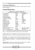
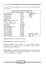
Page 40: ...isplay VGA EGA Password Check Setup Parity Check Disabled Boot To OS 2 DRAM 64MB or Above No ESC Exit Sel Wait For F1 If Error Enabled PgUp PgDn Modify Hit DEL Message Display Enabled F2 F3 Color Note The above page of the Advanced CMOS Setup only shows part of the related options To proceed to the next options please move your cursor downwards Advanced Setup options are displayed by choosing the ...

Page 41: ...press and runs WINBIOS Setup if the key has been pressed Enabled AMIBIOS does not test system memory above 1MB AMIBIOS does not wait up to 40 seconds for a READY signal from the IDE hard disk drive If a READY signal is not received immediately from the IDE drive AMIBIOS does not configure that drive AMIBIOS does not wait for 0 5 seconds after sending a RESET signal to the IDE drive to allow the ID...

Page 42: ...OS Cacheable Enabled C000 16k Shadow Disabled C400 16k Shadow Disabled C800 16k Shadow Disabled CC00 16k Shadow Disabled D000 16k Shadow Disabled D400 16k Shadow Disabled ESC Exit Sel D800 16k Shadow Disabled PgUp PgDn Modify DC00 16k Shadow Disabled F2 F3 Color Floppy Access Seek Predefined setting is Disabled HDD Access Control Predefined setting is Normal PS 2 Mouse Support When this option is ...

Page 43: ...RAM 64MB or Above Set this option to Yes to permit AMIBIOS to run with IBM OS 2 The settings are Yes or No The default settings are No Wait For F1 if Error AMIBIOS POST error messages are followed by Press F1 to continue If this option is set to Disabled AMIBIOS does not wait for you to press the F1 key after an error message The settings are Disabled or Enabled The Optimal and Fail Safe default s...

Page 44: ... 16K Shadow C800 16K Shadow D800 16K Shadow CC00 16K Shadow C000 16K Shadow These options control the location of the contents of the 16KB of ROM beginning at the specified memory location If no adaptor ROM is using the named ROM area this area is made available to the local bus The settings are Setting Description Shadow The contents of C0000h C3FFFh are written to the same address in system memo...

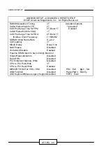
Page 45: ...Pulse Width When Refresh 6T DRAM Read Leadoff Time 1T RAMW Assertion Timing 3T CAS Pulse Width for FP 2T CAS Precharge Time for FPM 2T Burst 1T CAS Pulse Width for EDO 1T CAS Precharge Time for EDO 2T Burst 1T ISA Bus Clock Frequency 7 159MHZ SDRAM Write Retire Rate X 2 2 2 CAS Latency 3T MDLE Delay Delay 3 ns NA Enable Disabled ESC Exit Sel Write NA Disable Enabled PgUp PgDn Modify Pipeline SRAM ...

Page 46: ...or EDO 2T Burst 1T ISA Bus Clock Frequency 7 159MHZ SDRAM Write Retire Rate X 2 2 2 CAS Latency 3T MDLE Delay Delay 3 ns NA Enable Disabled Write NA Disable Enabled Pipeline SRAM back to back timing1 Bank L2 Single Read Allocation Disabled Read FIFO Disabled PCI Enhanced Memory Write Disabled CPU to PCI Post Write 3T CPU to PCI Burst Write Enabled MEMORY HOLE at 15M 16M Disabled ESC Exit Sel USB F...

Page 47: ...spend Standby Time Out Minute Disabled Suspend Time Out Minute Disabled Slow Clock Ratio 1 8 Ring Active Disabled IRQ 3 COM2 COM4 Monitor IRQ 4 COM1 COM3 Monitor IRQ 5 LPT2 Ignore IRQ 7 LPT1 Ignore IRQ 9 Ignore IRQ10 Ignore IRQ11 Ignore IRQ12 PS2 Mouse Monitor IRQ13 Math Coprocessor Ignore ESC Exit Sel IRQ14 Monitor PgUp PgDn Modify IRQ15 Monitor F2 F3 Color Power Management Setup options are disp...

Page 48: ...d The settings are Disabled Standby or Suspend The default settings are Disabled Standby Time Out Minute This option specifies the length of the period of system inactivity when the computer is in Full On mode before the computer is placed in Standby mode In Standby mode some power use is curtailed The settings are Disabled 1 Min 2 Min and all one minute intervals up to and including 15 Min The de...

Page 49: ...y AMIBIOS When any activity occurs the computer enters Full On mode Each of these options can be set to Monitor or Ignore The default setting for all options is Ignore l IRQ3 COM2 COM4 Monitor l IRQ4 COM1 COM3 Monitor l IRQ5 LPT2 Ignore l IRQ7 LPT1 Ignore l IRQ9 Ignore l IRQ10 Ignore l IRQ11 Ignore l IRQ12 PS2 Mouse Monitor l IRQ13 Math Coprocessor Ignore l IRQ14 Monitor l IRQ15 Monitor ...

Page 50: ...ity Auto PCI Slot2 IRQ Priority Auto PCI Slot3 IRQ Priority Auto PCI Slot4 IRQ Priority Auto DMA Channel 0 PnP DMA Channel 1 PnP DMA Channel 3 PnP DMA Channel 5 PnP DMA Channel 6 PnP ESC Exit Sel DMA Channel 7 PnP PgUp PgDn Modify IRQ3 ISA EISA F2 F3 Color PCI PnP Setup options are displayed by choosing the PCI PnP Setup icon from the WINBIOS Setup main menu All PCI PnP Setup options are described...

Page 51: ...the motherboard where the offboard PCI IDE controller card is installed If an offboard PCI IDE controller is used the onboard IDE controller on the motherboard is automatically disabled The settings are Disabled Auto Slot1 Slot2 Slot3 or Slot4 If Auto is selected AMIBIOS automatically determines the correct setting for this option The Optimal and Fail Safe default settings are Auto In the AMIBIOS ...

Page 52: ... PnP DMA Channel 6 PnP DMA Channel 7 PnP IRQ3 ISA EISA IRQ4 ISA EISA IRQ5 PCI PnP IRQ7 ISA EISA IRQ9 PCI PnP IRQ10 PCI PnP IRQ11 PCI PnP IRQ12 PCI PnP IRQ14 PCI PnP IRQ15 PCI PnP ESC Exit Sel Reserved Memory Size Disabled PgUp PgDn Modify Reserved Memory Address C8000 F2 F3 Color PCI Slot1 Slot2 Slot3 Slot4 IRQ Priority Without prior definition from the system board designer the default settings o...

Page 53: ...efault settings are PnP Reserved Memory Size This option specifies the size of the memory area reserved for legacy ISA adapter cards The settings are Disabled 16K 32K or 64K The optimal and Fail Safe default settings are Disabled Reserved Memory Address This option specifies the beginning address in hex of the reserved memory area The specified ROM memory area is reserved for use by legacy ISA ada...

Page 54: ...tion Disabled ESC Exit Sel Mouse Wake up function Disabled PgUp PgDn Modify Onboard PCI IDE Primary F2 F3 Color Peripheral Setup options are displayed by choosing the Peripheral Setup icon from the WINBIOS Setup main menu All Peripheral Setup options are described in this section Onboard FDC This option enables the floppy drive controller on the motherboard The settings are Enabled or Disabled The...

Page 55: ...1284 specifications The default setting is Normal The other settings are Setting Description Normal Normal The normal parallel port mode is used This is the default setting Cache Bi Dir Use this setting to support bidirectional transfers on the parallel port EPP The parallel port can be used with devices that adhere to the Enhanced Parallel Port EPP specification EPP uses the existing parallel por...

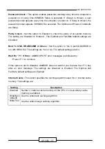
Page 56: ...i Virus Two Levels of Passwords Both the Supervisor and the User icons configure password support If you use both the Supervisor password must be set first The system can be configured so that all users must enter a password every time the system boots or when WINBIOS Setup is executed using either or both the Supervisor password or User password American AMIBIOS Setup Megatrends 1994 American Meg...

Page 57: ... when the password prompt appears Changing a Password Select the Supervisor or User icon from the Security section of the WINBIOS Setup main menu Enter the password and press Enter The screen does not display the characters entered After the new password is entered retype the new password as prompted and press Enter If the password confirmation is incorrect an error message appears If the new pass...

Page 58: ...ferent languages 3 11 BIOS DEFAULTS The icons of BIOS Defaults in this section permit you to select a group of settings for all WINBIOS Setup options Not only can you use these icons to quickly set system configuration parameters you can choose a group of settings that have a better chance of working when the system is having configuration related problems Original Choose the Original icon to retu...

Page 59: ...igger the Watch Dog timer 443H Step 2 Disable 43H EX 1 For DOS Execute the DEBUG EXE file under DOS Then key in i443 The system will reboot automatically according to the time out you set C DOS DEBUG i443 EX 2 For assemble Language Enable MOV DX 443H IN AL DX Disable IN AL 43H APPENDIX A ...

Page 60: ...F DMA Controller 2 0F0 0F1 Clear Reset Math Coprocessor 1F0 1F7 Hard Disk Controller 200 210 Game Port 278 27F Parallel Port 2 2E8 2EF Serial Port 4 COM 4 2F8 2FF Serial Port 2 COM 2 300 31F prototype Card Streaming Tape Adapter 360 36F PC Network 378 3FF Parallel Port 1 380 38F SDLC 2 3A0 3AF SDLC 1 3B0 3BF MDA Video Card Including LPTO 3C0 3CF EGA Card 3D0 3DF CGA Card 3E8 3EF Serial Port 3 COM ...

Page 61: ...loppy Disk Controller DMA 3 ECP Parallel Port DMA 4 Cascade for DMA 1 DMA 5 Reserved DMA 6 Reserved DMA 7 Reserved INTERRUPT CONTROLLER IRQ Function IRQ 0 System timer output IRQ 1 Keyboard IRQ 2 Cascade for INTC 2 IRQ 3 Serial port 2 IRQ 4 Serial port 1 IRQ 5 Parallel port 2 IRQ 6 Floppy disk controller IRQ 7 Parallel port 1 IRQ 8 Real time clock IRQ 9 Software redirected to INT 0AH IRQ 2 IRQ 10 ...

Page 62: ...e on AP 545L Single Board Computer Step 1 Plug the Dual Side Male Connector into the PC 104 female connector Step 2 Plug the PC 104 module s female connector into the AP 545L male connector PCI Module PCI Female Connector AP 545L Single Board Computer Dual Side Male Connector APPENDIX C ...

Page 63: ...epeater Adapter It is also called an expansion board expansion card or adapter card It is a small circuit board that is installed in the expansion slots on the motherboard You can install a particular adapter that connects a new device such as internal modem sound card and scanner AGP Advanced Graphic Port is a new 32 bit interface with external clock rate of 66MHz that transmit a maximum of 528MB...

Page 64: ...d controls the flow of data providing the brain that enables the PC to calculate and perform the operations like sorting information more quickly than a human could The CPU makes perhaps the greatest contribution to a PC s speed and power Note Any additional information is subject to change without prior revision from the supplier Table 1 CPU Speeds Processor type Speed ratings MHz 486DX2 66 80 48...

Page 65: ...professional society that issues its own standard and is a member of ANSI and ISO Popular known standards is IEEE802 3 is a physical layer standard for 10Base T 100Base T Ethernet and StarLAN IEEE802 5 is a physical layer standard for Token Ring IEEE802 11 is a physical layer standard for Wireless LAN WAN compatibility IEEE802 12 is a physical layer standard for 100VG AnyLAN LAN Local Area Network...

Page 66: ...ed more awkward methods of navigating with the keyboard Digitizing tablets are popular with architects and engineers who must translate precise movements of a pen into lines on the screen Touch screens on which you press either your finger and a special light pen to control the software are too tiring to use for any length of time MMXÔ CPU s with MMXÔ technology are optimized to run multimedia app...

Page 67: ...are saved to a disk RAM forgets them when you turn your computer off RAM is measured in megabytes M Most computers today come with 32M of RAM though some sell with only 16M installed There are a few different flavors and speeds of RAM as well One of the most prominent today is Extended Data Output EDO RAM but an even faster type of RAM that has just hit the market is called SyncDRAM Serial port Se...

Page 68: ...use and game ports into one asynchronous and isochronous communications port with bandwidth for data transfer speeds up to 12 Mbps without termination By daisy chaining USB hubs up to 127 I O devices can be connected to one USB port on the PC USB is completely plug and play meaning peripherals can be correctly detected and configured automatically as soon as they are connected UTP Unshielded Twist...

Page 69: ...eturned at the customer expense 5 The following conditions are excluded from this warranty A Improper or inadequate maintenance by the customer B Unauthorized modification or misuse C Operation outside of the environmental specifications for the product RMA Service 1 Request a RMA Complete and fax to Supplier the RMA Request Form to obtain a RMA number 2 Shipping A The customer is requested to fil...

Page 70: ... Return Shipping Address For Supplier only RMA No Account Sales Model No Serial No Problem Code Remark This form could be copied for more description Problem Code 01 D O A 02 Second Time R M A 03 No Screen 04 CMOS Data Lost 05 FDC Fail 06 HDC Fail 07 Bad Slot 08 BIOS Problem 09 Keyboard Controller Fail 10 Cache RMA Problem 11 Memory Socket Bad 12 Hang Up Hardware 13 Hang Up Software 14 Other Pls S...

Reviews: