background image

Appendix C: Programming Generation 2 LAN Bypass


55 


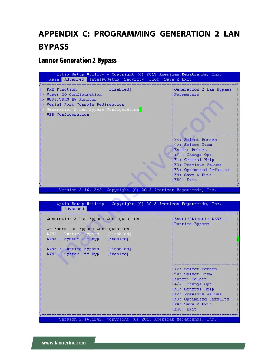
Lanner Generation 2 bypass is configured through the BIOS menu as shown below: 


Summary of Contents for FW-7551SE

Page 1: ...1 FW 7551SE User Manual Version 1 0 Date of Release 2018 08 13 Network Computing...

Page 2: ...facturer Information provided in this manual is intended to be accurate and reliable However the original manufacturer assumes no responsibility for its use nor for any infringements upon the rights o...

Page 3: ...sure compliance of this unit to the specified limits of the rules This device complies with part 15 of the FCC rules Operation is subject to the following two conditions 1 this device may not cause ha...

Page 4: ...not achieved due to uneven mechanical loading Circuit Overloading Consideration should be given to the connection of the equipment to the supply circuit and the effect that overloading of the circuits...

Page 5: ...placement de composants Portez un bracelet anti ESD et veillez ce qu il soit bien au contact de la peau Si aucun bracelet n est disponible reliez votre corps la terre en touchant la partie m tallique...

Page 6: ...FW 7551SE User Manual 6 Version Date Descriptions 1 0 2018 08 13 1 st Release...

Page 7: ...Hardware Installation 24 Installing the System Memory 26 Installing the M 2 Interface LTE Module and Storage Module 27 Installing the MPCIE Interface LTE Module 29 Installing the Wireless Module 31 I...

Page 8: ...FW 7551SE User Manual 8 Lanner Generation 2 Bypass 55 Warranty Policy 58 RMA Service 58 RMA Service Request Form 59...

Page 9: ...IM Slots 1x 2 5 HDD SSD Bay Optional Note For instructions on quick installation and acquiring the Intel Atom Processor C2000 Product Family for Communications Infrastructure Software for Linux Softwa...

Page 10: ...FW 7551SE User Manual 10...

Page 11: ...Console 1x RJ45 USB 2x USB 2 0 LCD Module N A Display N A Power input 1x DC Jack Storage HDD SSD Support 1x 2 5 Bay Optional Onboard Storage 1x CFAST Expansion PCIe N A mini PCIe 1x Mini PCIe PCIe USB...

Page 12: ...red it indicates that the system is malfunctioning HDD If the LED blinks it indicates data access activities otherwise it remains off Speed Link Activity These LEDs are indicators for the 4 or 6 by SK...

Page 13: ...top bit no flow control R6 USB Port 2x USB 2 0 ports F7 SFP Ports 2x SFP ports F8 GbE Ports 4x GbE ports 4 or 6 by SKU on board Ethernet ports equip with 2 pairs of LAN bypass These 4 GbE ports are pr...

Page 14: ...FW 7551SE User Manual 14 The block diagram indicates how data flows among components on the motherboard Please refer to the following figure for your motherboard s layout design...

Page 15: ...nnectors and jumpers on the board Refer to the following picture as a reference of the pin assignments and the internal connectors J4 JBAT1 PS4P1 SATS6G_1 SPIROM1 MPCIE1 JMINI_LED1 NGFF1_LTE NGFF2_STO...

Page 16: ...FW 7551SE User Manual 16 SIM1_PCIE SIM2_LTE...

Page 17: ...es such as no master slave designation for SATA devices each device is treated as a master and hardware assisted native command queuing AHCI also provides usability enhancements such as Hot Plug You w...

Page 18: ...KE 2 P3V3_MINI 3 NC 4 GND 5 NC 6 P1V5 7 MINI_CLKREQ_N1 8 UIM1_PWR 9 GND 10 UIM1_DAT 11 MINIPCIE_REFCLKN 12 UIM1_CLK 13 MINIPCIE_REFCLKP 14 UIM1_RST 15 GND 16 UIM1_VPP 17 NC 18 GND 19 NC 20 RF_KILL_N2_...

Page 19: ...I 75 NC 1 GND_PRESENCE_IND GND 3 3V3_AUX2 GND 5 3V3_AUX4 USB2_D F_CARD_PWROFF USB2_D W_DIS GND 11 LED 1DAS DSS NOTCH 1 NOTCH 5 NOTCH 2 NOTCH 6 NOTCH 3 NOTCH 7 NOTCH 4 NOTCH 8 AUDIO_0 GND WWAN OC SSD A...

Page 20: ...3V3_MINI 75 NC 1 GND_PRESENCE_IND GND 3 3V3_AUX2 GND 5 3V3_AUX4 USB2_D F_CARD_PWROFF USB2_D W_DIS GND 11 LED 1DAS DSS NOTCH 1 NOTCH 5 NOTCH 2 NOTCH 6 NOTCH 3 NOTCH 7 NOTCH 4 NOTCH 8 AUDIO_0 GND WWAN O...

Page 21: ...et mode when the reset switch is pressed The hardware reset will reboot the system without turning off the power The software reset can be programmed to reset a software to its default setting Pin Des...

Page 22: ...DDR3 1333 1600 ECC memory The system can support up to 8 GB in maximum AT Mode Power Button Connector J21 Pin Description 1 LAN1_LINK_ACT_N 2 LAN1_LINK_100_N Pin Description 1 LAN2_LINK_ACT_N 2 LAN2_L...

Page 23: ...PCIE SIM2_LTE SIM CONN_6P For M 2 Pin Description Pin Description C1 UIM1_PWR C4 UIM1_DATA C2 UIM1_RST C5 UIM1_VPP C3 UIM1_CLK C6 GND Pin Description Pin Description C1 UIM2_PWR C4 UIM2_DATA C2 UIM2_...

Page 24: ...tain service procedures you must perform the following procedures first WARNING To reduce the risk of personal injury electric shock or damage to the equipment remove the power cord to remove power fr...

Page 25: ...Chapter 3 Hardware Setup 25 3 Slide the cover backwards to open it...

Page 26: ...et the higher bandwidth requirements of the latest operating system and Internet applications To install the memory 1 Open the DIMM slot latches 2 Install the DIMM Note The system requires DDR3 1333 1...

Page 27: ...cket key in the slot Insert the module at 30 degrees into the socket until it is fully seated in the connector 3 Push down on the module and secure it with the screw that comes with the package 4 For...

Page 28: ...rews that fix the cover of SIM card holder to reveal the SIM slots Insert the SIM card into SIM2_LTE slot and fix the cover with 2 screws 6 For LTE module Attach the LTE antennas onto the front panel...

Page 29: ...Align the notch of the module with the socket key in the slot Insert the module at 30 degrees into the socket until it is fully seated in the connector 3 Fix the module to the motherboard with screws...

Page 30: ...ews that fix the cover of SIM card holder to reveal the SIM slots Insert the SIM card into SIM1_MPCIE slot and fix the cover with 2 screws 6 Attach the LTE antennas onto the front panel Make sure the...

Page 31: ...e notch of the module with the socket key in the slot Insert the module at 30 degrees into the socket until it is fully seated in the connector 3 Fix the module to the motherboard with a screw 4 Snap...

Page 32: ...FW 7551SE User Manual 32 5 Attach the LTE antennas onto the front panel Make sure the antenna cables WIFI0 and WIFI1 go through the right holes as indicated in the picture WIFI1 WIFI0...

Page 33: ...ith 4 disk screws on the tray 4 Connect the Serial ATA power and data cables to the hard disk s power and drive connector respectively 5 Plug the Serial ATA power and data disk cables to the Serial AT...

Page 34: ...to run this program Press Delete during the Power On Self Test POST to enter the Setup utility There are a few cases that other keys may be used such as F1 F2 and so forth otherwise POST continues wit...

Page 35: ...4 Enter ESC Arrow keys and so on Control Keys Description The Left and Right Arrow keys allow you to select a setup screen For example Main screen Advanced screen Boot screen and so on The Up and Down...

Page 36: ...legend Above the key legend is an area reserved for a text message When an option is selected in the left frame it is highlighted in white Often a text message will accompany it The screenshots prese...

Page 37: ...he left frame of the screen such as SuperIO Configuration to go to the sub menu for that item You can display an Advanced BIOS Setup option by highlighting it using the Arrow keys All Advanced BIOS Se...

Page 38: ...you to boot computers using a network interface independently of data storage devices like hard disks or installed operating systems Enable or disable this function with this option here For LAN port...

Page 39: ...the serial port base address and the IRQ port Change Settings Selects the port base address and the IRQ port Item Description Parallel Port Enable or disable this parallel port Device Settings Shows t...

Page 40: ...temperatures CPUFAN0 Speed CPU FAN The onboard hardware monitor automatically detects and displays the CPU fan speeds in rotations per minute RPM If the fan is not connected to the motherboard it dis...

Page 41: ...Enable or disable BIOS through remote access Console Redirection Settings Enter to view more options Item Description Terminal Type Sets the connection terminal type Bits per second Data bits Parity...

Page 42: ...nable or disable the automatic activation of hardware LAN Bypass function in the event of a power failure Hardware Bypass can automatically activate to allow network traffic to continue The LAN bypass...

Page 43: ...BIOS Setup 43 Bypass settings in the BIOS System Status Runtime LAN Bypass for Module 1 Power off LAN Bypass for Module 1 Enabled Disabled Disabled Power on Non Bypass Non Bypass Power off Non Bypass...

Page 44: ...em is fully booted with all USB drivers loaded When this option is enabled any attached USB mouse or USB keyboard can be used on the system even when there is no USB drivers loaded on it It allows you...

Page 45: ...definitely until it is manually canceled or the transfer completes normally If set to a nonzero value time out interval the host controller starts a timer when it receives the transfer request When th...

Page 46: ...disable this feature CPU C State CPU operating states C states are the capability of an idle processor to turn off unused components to save power Enable or disable or set it to automatically switch t...

Page 47: ...Chapter 4 BIOS Setup 47 It shows the memory information such as the total detected memory and memory frequency...

Page 48: ...nu sets delay time for USB operations Item Selection Power Off When setting to Power Off the system goes into off state after an AC power interruption Power On When setting to Power on the system turn...

Page 49: ...d write requests are outstanding most often occurring in server type applications native command queuing It also facilitates hot swapping Disable Disable the SATA controller Item Selection Staggered S...

Page 50: ...nter the user password for booting and accessing the system however some functions may be disabled 1 To set an Administrator User password 2 Select the option item and press Enter 3 From the Create Ne...

Page 51: ...s for the boot setup prompt to wait for user s intervention during the POST Bootup Num Lock State This option lets you to enable or disable the function of the NumLock key Quiet Boot Enabling this ite...

Page 52: ...mputer so the new system configuration parameters can take effect Discard Changes and Reset This option allows you to discard the selections you made and restore the previously saved values After sele...

Page 53: ...functioning and the processor s reset signal is asserted Thus the processor will be restarted as if a human operator had cycled the power To execute the utility enter the number of seconds to start co...

Page 54: ...the console cable to console port of the system and the other end to the serial port of the Remote Client System 2 Configure the following settings in the BIOS Setup menu BIOS Advanced Serial Port Con...

Page 55: ...Appendix C Programming Generation 2 LAN Bypass 55 Lanner Generation 2 bypass is configured through the BIOS menu as shown below...

Page 56: ...for Module 1 Power off LAN Bypass for Module 1 Enabled Disabled Disabled Power on Non Bypass Non Bypass Power off Non Bypass Non Bypass 2 A watchdog timer can be used to control the LAN Bypass functi...

Page 57: ...ash Authenticate Operation Cipher Hash Combined Operation Key Derivation Operation Public Key Functions RSA Operation Diffie Helman Operation Digital Signature Standard Operation Key Derivation Operat...

Page 58: ...xpense 5 The following conditions are excluded from this warranty Improper or inadequate maintenance by the customer Unauthorized modification misuse or reversed engineering of the product Operation o...

Page 59: ...Appendix E Terms and Conditions 59 When requesting RMA service please fill out the following form Without this form enclosed your RMA cannot be processed...

Reviews: