background image

 
Chapter2 Installation 

16 

User’s Manual 

z

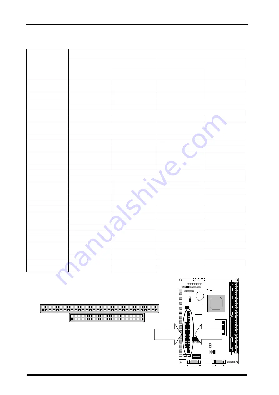
CONA1:PC/104 Connector

8 bit


z

CONB1:PC/104 Connector

16 bit


Description 

CONA1 CONB1 

Pin No. 

Row A 

Row B 

Row C 

Row D 

1 IOCHCK# 

Ground Ground Ground 

2 SD7 

RSTDRV 

SBHE# 

MEMCS16# 

3 SD6 +5V LA23 

IOCS16# 

4 SD5 IRQ9 LA22 

IRQ10 

5 SD4 -5V LA21 

IRQ11 

6 SD3 

DRQ2 LA20 

IRQ12 

7 SD2 -12V LA19 

IRQ15 

8 SD1 

WS# 

LA18 

IRQ14 

9 SD0 

+12V LA17 

DACK0# 

10 IOCHRDY  NC  MEMR# DRQ0 
11 AEN 

SMEMW# 

MEMW# 

DACK5# 

12 SA19 

SMEMR# 

SD8 DRQ5 

13 SA18 IOW# SD9 

DACK6# 

14 SA17 IOR# SD10 DRQ6 
15 SA16 

DACK3# 

SD11 

DACK7# 

16 SA15 DRQ3 SD12 DRQ7 
17 SA14 

DACK1# 

SD13 +5V 

18 SA13 DRQ1 SD14 

MASTER# 

19 SA12 

REFRESH# 

SD15 

Ground 

20 SA11 

SYSCLK NC Ground 

21 SA10 IRQ7  ---  --- 
22 SA9 IRQ6  ---  --- 
23 SA8 IRQ5  ---  --- 
24 SA7 IRQ4  ---  --- 
25 SA6 IRQ3  ---  --- 
26 SA5 

DACK2# ---  --- 

27 SA4  TC  ---  --- 
28 SA3 BALE  ---  --- 
29 SA2 +5V  ---  --- 
30 SA1 OSC  ---  --- 
31 SA0 

Ground ---  --- 

32 Ground 

Ground 

---


---


32 
32


CONB1 

20 
20


C 1 
D 1


B 1 
A 1

CONA1 


CONB1 

CONA1 

Summary of Contents for IAC-H488 Series

Page 1: ...IAC H488 Series Half size 486 SBC with VGA LAN CompactFlash STPC Consumer II 133CPU User s Manual...

Page 2: ......

Page 3: ...d by the purchaser for backup purposes All rights reserved TRADEMARKS Pentium Celeron are registered trademark of Intel Corporation The following are trademarks or registered trademarks of their respe...

Page 4: ......

Page 5: ...Chapter 3 BIOS Setup 19 3 1 Running AMI BIOS 19 3 2 AMI BIOS HIFLEX Setup Utility 20 3 3 Standard CMOS Setup 21 3 4 Advanced CMOS Setup 22 3 5 Advanced Chipset Setup 25 3 6 Power Management Setup 27...

Page 6: ......

Page 7: ...ompactFlash socket in the rear supports ATA mode Type I II Enhanced IDE interface two serial ports RS 232 and RS 232 422 485 with DB 9 connector as COM1 and a mini DIN PS 2 keyboard mouse interface Th...

Page 8: ...in PC 104 expansion bus External Power Connector 4 pin external power connector Watchdog Timer 16 level time out intervals Operating Temperature 0 C 60 C Storage Temperature 20 C 70 C Humidity 5 95 no...

Page 9: ...Chapter1 Introduction 3 User s Manual 1 5 Board Layout...

Page 10: ...l Chapter 2 Installation 2 1 Hardware Setup and Installation 2 1 1 System Memory Installation Step1 Open latches of DIMM socket Step2 Insert the RAM module into the DIMM socket Step3 Press the latches...

Page 11: ...ors 2 2 1 Board Outline of IAC H488 1 KBPW1 1 1 1 1 1 1 VGAA1 COMA1 LANB1 PKMA1 IRDA1 1 ATXC1 KCN1 COMB1 1 11 PLRS1 2 PSW1 1 1 3 4PSM1 SC2T1 5 6 1 2 9 1 4 12 SC2T2 ISP1 1 1 1 5 3 3 JFA2 JFA1 COMS1 1 C...

Page 12: ...rogramming JFA1 JFA2 Default 1 2 Program 2 3 z SC2T1 SC2T2 Select COM2 Type COM2 Type SC2T1 SC2T2 RS 232 Default 1 2 1 5 2 6 3 7 4 8 RS 422 3 4 5 9 6 10 7 11 8 12 RS 485 5 6 5 9 6 10 7 11 8 12 SC2T1 1...

Page 13: ...BPW1 1x3 Pin 2 54mm PS 2 Keyboard Mouse KBPW1 5V Default 1 2 5V STANDBY 2 3 z CMOS1 Clear CMOS Data Description CMOS1 Normal Default 1 2 Clear CMOS 2 3 1 KBPW1 Clear CMOS1 Normal Default CMOS1 3 2 1 C...

Page 14: ...for Power LED Reset Speaker Connector HD LED COMB1 Serial Port 2 Connector Header LANB1 LAN Connector VGAA1 VGA Connector LPTA1 Parallel Port Connector Header IDEB1 IDE Interface Connector Header KCN...

Page 15: ...SP 5 NC 6 MODE 7 Ground 8 SCLK z COMA1 RS 232 Serial Port 1 Connector D Sub Pin No Description 1 Data Carrier Detect DCDA 2 Receive Data RXDA 3 Transmit Data TXDA 4 Data Terminal Ready DTRA 5 Ground G...

Page 16: ...DB Transmit Data TXD Data 4 Request To Send RTSB NC NC 5 Transmit Data TXDB Receive Data RXD NC 6 Clear To Send CTSB NC NC 7 Data Terminal Ready DTRB Receive Data RXD NC 8 Ring Indicator RIB NC NC 9 G...

Page 17: ...lect A 15 Ground 16 Motor Enable B 17 Ground 18 Direction 19 Ground 20 Step 21 Ground 22 Write Data 23 Ground 24 Write Gate 25 Ground 26 Track 0 27 Ground 28 Write Protect 29 NC 30 Read Data 31 Ground...

Page 18: ...ription 1 PANSW 2 GND z PLRS1 Power LED Reset Speaker Connector Pin No Description 1 Power LED 2 Power LED 3 GND 4 HDD LED 5 HDD LED 6 RESET SW 7 RESET SW GND 8 External Speaker 9 Internal Buzzer 10 N...

Page 19: ...Sync 15 DDC CLK z LPTA1 Parallel Port Connector Header Pin No Description Pin No Description 1 Strobe 2 Auto Form Feed 3 Data 0 4 Error 5 Data 1 6 Initialize 7 Data 2 8 Printer Select In 9 Data 3 10...

Page 20: ...Data 9 7 Data 5 8 Data 10 9 Data 4 10 Data 11 11 Data 3 12 Data 12 13 Data 2 14 Data 13 15 Data 1 16 Data 14 17 Data 0 18 Data 15 19 Ground 20 NC 21 DMA REQ 22 Ground 23 IOW 24 Ground 25 IOR 26 Groun...

Page 21: ...Description 1 Ground 2 5V Standby 3 Ground 4 Power ON z IRDA1 Consumer Remote Control IR CIR Pin No Description 1 5V 2 NC 3 IRRX 4 GND 5 IRTX IRDA1 1 5 ATXC1 4 1 Note To have full features from ATX p...

Page 22: ...IRQ15 8 SD1 0 WS LA18 IRQ14 9 SD0 12V LA17 DACK0 10 IOCHRDY NC MEMR DRQ0 11 AEN SMEMW MEMW DACK5 12 SA19 SMEMR SD8 DRQ5 13 SA18 IOW SD9 DACK6 14 SA17 IOR SD10 DRQ6 15 SA16 DACK3 SD11 DACK7 16 SA15 DR...

Page 23: ...DATA13 5 DATA6 30 DATA14 6 DATA7 31 DATA15 7 CE1 32 CE2 8 A10 33 VS1 9 OE 34 IOR 10 A9 35 IOW 11 A8 36 WE 12 A7 37 READY 13 CFVCC 38 CFVCC 14 A6 39 CSEL 15 A5 40 VS2 16 A4 41 RESET 17 A3 42 WAIT 18 A...

Page 24: ...Chapter2 Installation 18 User s Manual z z z zDIMMA1 168 Pin DIMM Connector DIMMA1 DIMMA1...

Page 25: ...rd hardware If the routines encounter an error during the tests the error will be reported in either of the two different ways 1 hear a series of short beeps or 2 see an error message on the screen di...

Page 26: ...displayed at the bottom of the screen ESC Exit the utility Use arrow keys to move cursor to your desired selection F2 F3 Changes background and foreground colors F10 Saves all changes made to Setup an...

Page 27: ...Sel PgUp PgDn Modify F1 Help F2 F3 Color Standard CMOS Setup options are displayed by choosing the Standard field from the AMIBIOS HIFLEX SETUP menu All Standard Setup options are described below Date...

Page 28: ...ite Hard Disk Access Control Read Write S M A R T for Hard Disks Enabled BootUp Num Lock On Floppy Drive Swap Disabled Floppy Drive Seek Disabled PS 2 Mouse Support Enabled Primary Display VGA EGA Pas...

Page 29: ...m to try to boot from other devices if the system fails to boot from the 1st 2nd 3rd Boot Device Floppy Access Control This option specifies the read write access that is set when booting from a flopp...

Page 30: ...tents of the F0000h system memory segment can be read from or written to L2 secondary cache memory The contents of the F0000h memory segment are always copied from the BIOS ROM to system RAM for faste...

Page 31: ...m board designer Any attempt to change the parameter of the fields are not recommended VGA Frame Buffer Size KB This option help you to use a VGA frame buffer and 16 Mb of RAM at the same time the sys...

Page 32: ...ead cycles from PCI to host are allowed to complete before the PCI cycle is terminated and all burst read attempts will be disconnected on the PCI bus PCI to Host Write Posting If enabled all QWORD al...

Page 33: ...led will activate the Advanced Power Management APM feature to enhance power saving modes Settings Enabled and Disabled Video Power Down Mode This option specifies the power conserving state that the...

Page 34: ...Activity This option allows you to enable event monitoring on the keyboard If set to Monitor and the computer is in a power saving state AMIBIOS watches for keyboard activity The computer enters the...

Page 35: ...d in this section Plug and Play Aware O S Set this option to Yes if the operation system installed in the computer is Plug and Play aware BIOS only detects and enables PnP ISA adapter cards that are r...

Page 36: ...A OnBoard IDE Both ESC Exit Sel PgUp PgDn Modify F1 Help F2 F3 Color Peripheral Setup options are displayed by choosing the Peripheral Setup icon from the AMI BIOS Setup main menu All Peripheral Setu...

Page 37: ...ECP uses the DMA protocol to Achieve transfer rates of approximately 2 5 Mbs ECP provides symmetric Bidirectional communications EPP Version This option is only valid if the Parallel Port Mode option...

Page 38: ...Precompensation Cylinder Older hard drives have the same number of sectors per track at the innermost tracks as at the outermost tracks This means that the data density at the innermost tracks is high...

Page 39: ...You will be prompted to confirm the password Retype the password and press Enter You may also press Esc to abort the selection and not enter a password To clear a set password just press Enter when yo...

Page 40: ...ate hard disk type etc ESC Exit Sel F2 F3 Color F10 Save Exit Pressing Y loads the defaults BIOS values 3 12 Save Exit Setup When you want to quit the Setup menu you can select this option to save the...

Page 41: ...rd CMOS Setup Advanced CMOS Setup Advanced Chipset Setup Power Management Setup PCI Plug and Play Setup PCI Plug and Play Setup Peripheral Setup Hardware Monitor Setup Auto Detect Hard Disks Change Us...

Page 42: ...install the drivers in generally and related directory that come with the CD ROM in the package Please follow the instructions set forth on the screen carefully 1 Find the directory for your O S acco...

Page 43: ...lecting hardware or software watch dog if both of them are available Software setting period normally setting watch dog timer period to 16 level Software watch dog using example EX 1 For DOS Enable Di...

Page 44: ...will be returned at the customer expense 5 The following conditions are excluded from this warranty A Improper or inadequate maintenance by the customer B Unauthorized modification or misuse C Operat...

Page 45: ...Item Model Name Serial Number Configuration Item Problem Code Failure Status Problem Code 01 D O A 02 Second Time R M A 03 CMOS Data Lost 04 FDC Fail 05 HDC Fail 06 Bad Slot 07 BIOS Problem 08 Keyboar...

Reviews: