ICS-P570 User Manual
14
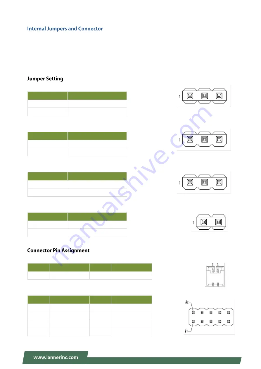
The pin headers on the motherboard are often associated with important functions. With the shunt (Jumper)
pushed down on the designated pins (the pin numbers are printed on the circuit board, surrounding the pin
header), certain feature can be enabled or disable. When changing the jumpers, make sure your system is
completely turned off.
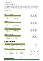
1. J10
: LPC1114 Burn Select
Jumper
Description
1-2 (Default)
Normal
2-3
Burn Mode
2. JCMOS1
: Clear CMOS
Jumper
Description
1-2 (Default)
Normal
2-3
Clear CMOS RAM
3. SEL1
: Hardware / Software Select
Jumper
Description
1-2
Software Reset
2-3 (Default)
Hardware Reset
4. PWR1: Power On / Off
Jumper
Description
1-2
Power On/Off
2-3 (Default)
Normal
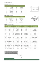
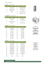
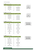
1. BAT1
: Battery Connector
Pin No.
Description
Pin No.
Description
1
VDD_3.3V_BAT
2
GND
2. JSPI1
: SPI ROM Pin Header
Pin No.
Description
Pin No.
Description
1
V1P8_A_SPI
2
GND
3
SPI0_CS_N
4
SPI0_CLK
5
SPI0_MISO
6
SPI0_MOSI
7
NC
8
SPI0_HOLD_#
Summary of Contents for ICS-P570
Page 12: ...ICS P570 User Manual 12 No Description B1 SD SIM Cover SD Card Dual Nano SIM Card Cover B1 ...
Page 13: ...ICS P570 User Manual 13 ...
Page 22: ...ICS P570 User Manual 22 4 Lift the cover to remove ...
Page 27: ...ICS P570 User Manual 27 3 Screw the two 2 antennas to the system ...
Page 38: ...ICS P570 User Manual 38 ...
Page 39: ...ICS P570 User Manual 39 ...
Page 40: ...ICS P570 User Manual 40 ...
Page 45: ...ICS P570 User Manual 45 ...
Page 46: ...ICS P570 User Manual 46 Node 0 Information ...
Page 53: ...ICS P570 User Manual 53 ...
Page 54: ...ICS P570 User Manual 54 ...


