CHAPTER 2: MOTHERBOARD INFORMATION
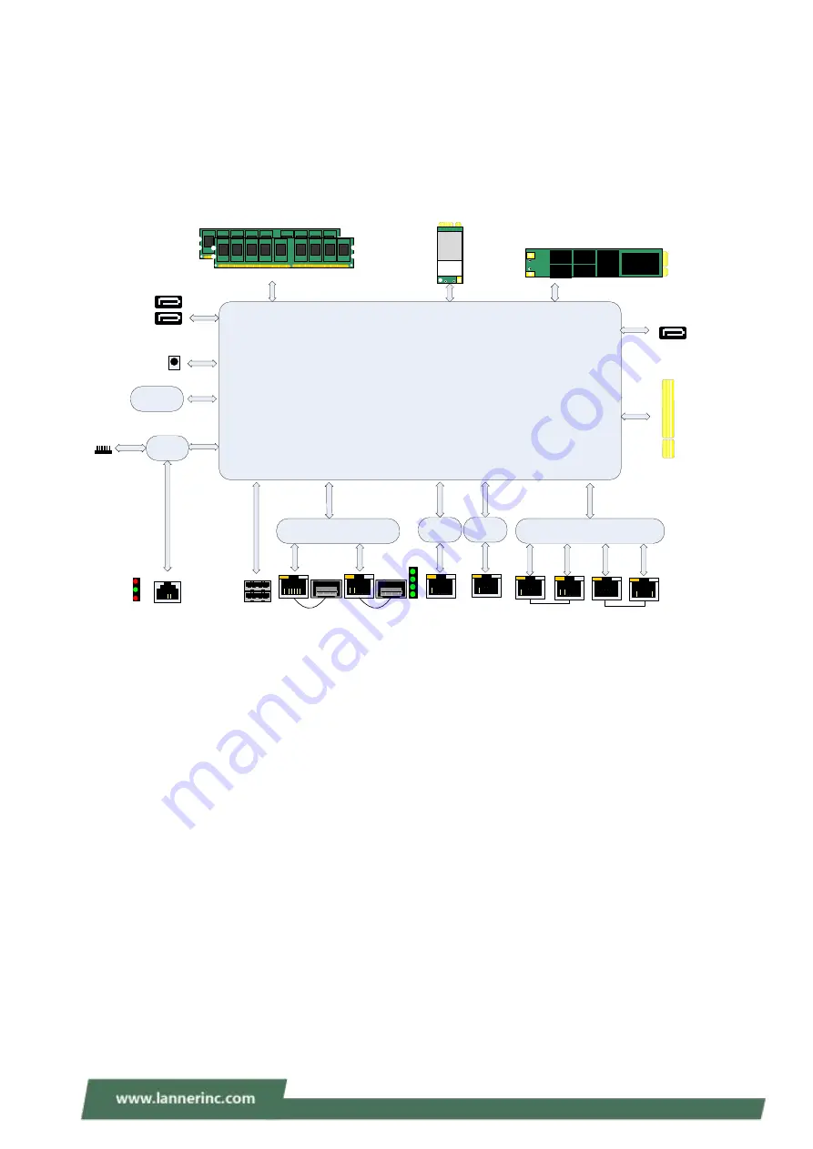
Block Diagram
The block diagram indicates how data flows among components on the motherboard. Please refer to the
following figure for your motherboard’s layout design.
Intel Denverton-NS
8C C3758(20 HSIO)/ 4C 3558R(20 HSIO) /2C 3338R(10 HSIO)
DDR4
G
P
IO
USB2.0/3.0
RJ-45
Console
Reset Bottom
S
A
T
A
3.0
Support upto 64GB ECC/non-ECC
DDR4 Long-DIMM (2DPC)
SATA3.0
I210AT
1x PCIEx1
1x PCIEx1
TPM2.0
L
P
C
U
S
B
3.
0
88E1543
4x SGMII
I210AT
SIO
SLB9670VQ
One pair
Gen3
bypass
2
nd
console
MiniPCIE
1xPCIE/USB2.0
One pair
Gen3
bypass
USB2.0
S
P
I
I350-AM2
1x PCIEx2
Support PGN Module(USB 3.0 Signal)
1x
P
C
IE
x8
o
r
2
x
P
C
IE
x4
M.2 2280 SATA SSD
colayout
colayout
USB 3.0SKU A/B only


