NCA-5220 User Manual
18
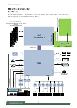
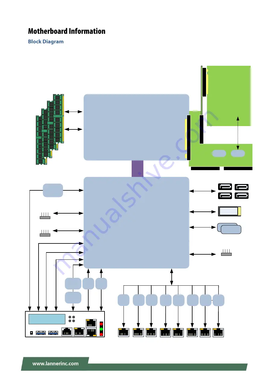
The block diagram indicates how data flows among components on the motherboard. Please refer to the
following figure for your motherboard’s layout design.
C246
I210-
AT
I210-
AT
I210-
AT
I210-
AT
I210-
AT
I210-
AT
I210-
AT
I210-
AT
Bypass
Bypass
Bypass
PCIe x1 *8
Intel
Coffee Lake-S
DDR4 Non-ECC (ECC) 2666Mhz
Dual Channel, 2x DIMM Sockets from Each Channel
Up to 128GB
(ECC supported with C246 PCH)
MUX
DMI Gen3
SATAIII
SATAIII
M.2
Support Upper Layer
(NM-4010IG401A)
P
C
Ie
x
1
*
4
LPC
BIOS
I210-
AT
PCIE x8
PCIE x8 or 2* PCIE x4
(Share with Rear PCIE)
P
C
IE
x
1
6
o
r
2
*
P
C
IE
x8
O
r
1
*
P
C
IE
x
8
+
2
*
P
C
IE
x
4
2
* P
C
IE
x
4
P
C
IE
x
8
o
r
2
*
P
C
IE
x
4
(S
h
ar
e
w
/
N
IC
2
)
HDMI
I210-
AT
I2C
PCIe x1 *2
LC
M
(S
er
ia
l P
o
rt
)
USB 3.0
USB Pin Header
USB 2.0
LPC
TPM
Super IO
LE
D
a
n
d
C
o
n
so
le
GPIO
R
es
et
B
o
tt
o
m
OPMA
MUX
LCM Module
REALTEK
RTL8211E
SPI
BIOS
Summary of Contents for NCA-5220
Page 62: ...NCA 5220 User Manual 62 CPU Configuration...
Page 69: ...NCA 5220 User Manual 69 Trusted Computing TPM2 0...
Page 71: ...NCA 5220 User Manual 71 Super IO Configuration...
Page 84: ...NCA 5220 User Manual 84 Intel TXT Information...
Page 90: ...NCA 5220 User Manual 90 NVMe Configuration...
Page 94: ...NCA 5220 User Manual 94 Memory Configuration...
Page 96: ...NCA 5220 User Manual 96 PEG Port Configuration...
Page 100: ...NCA 5220 User Manual 100 PCI Express Configuration...


