MIPI D-PHY Bandwidth Matrix Table
User Guide
© 2015-2018 Lattice Semiconductor Corp. All Lattice trademarks, registered trademarks, patents, and disclaimers are as listed at
All other brand or product names are trademarks or registered trademarks of their respective holders. The specifications and information herein are subject to change without notice.
24
FPGA-UG-02041-1.1
7.2.3.
ECP5/ECP5-5G
Maximum MIPI compliance data rate calculation for ECP5/ECP5-5G:
0.183 = 0.15 x UI
UI = 0.183/0.15 = 1.22 ns
Max Data Rate = 1/UI = 1/1.22 = 820 Mbps (at 0.15 UI)
Setup Time
Hold Time
0.442
0.442
At 800 Mbps, ½ UI = 0.625
Tskew = 0.625 - 0.442 = 0.183
ECP5/ECP5-5G Data Sheet Rev. 1.9 at 800 Mbps
Generic DDRX2 Outputs with Clock and Data Centered at Pin (GDDRX2_TX.ECLK.Centered) Using PCLK Clock Input, Left and Right Sides Only
t
SU_GDDRX2_centered
Data Output Valid Before CLK Output
t
HD_GDDRX2_centered
f
DATA_GDDRX2_centered
GDDRX2 Data Rate
f
MAX_GDDRX2_centered
GDDRX2 CLK Frequency (ECLK)
0.442
—
800
400
—
—
—
0.442
0.56
—
700
350
—
—
—
0.56
0.676
—
624
312
—
—
—
0.676
Mb/s
MHz
ns + ½ UI
Data Output Valid After CLK Output
All Devices
All Devices
All Devices
All Devices
ns + ½ UI
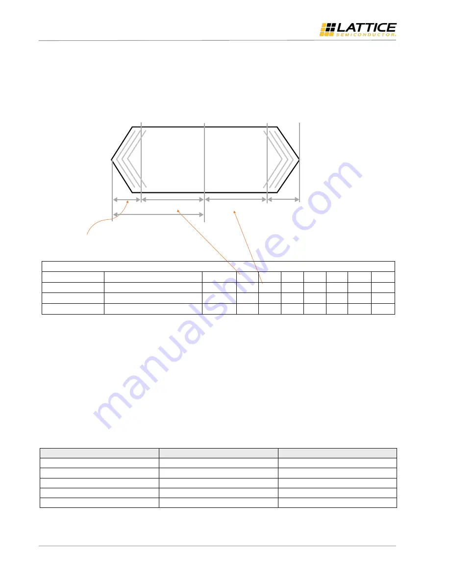
Figure 7.7. ECP5/ECP5-5G Maximum Data Rate
7.2.4.
Tskew Window at Higher Data Rate
For data rate higher than specified above, the tskew window may exceed the 0.15UI specified in the MIPI Alliance
Specification.
To calculate the window, the following equation can be used:
½ UI = ½ * (1 / Data Rate)
Tskew Window = (½ UI – min (tDVA, tDVB) / UI)
For 800 Mbps, 1 / Data Rate = 1.25 ns.
The maximum data rate each device can support on the receiver is limited to the data rate supported with
IDDRX2/X4/X8 with center-aligned data. This can be summarized in
Table 7.2. Tskew Window for Higher Data Rate
Device Family
Max Data Rate
Tsu/Thd Window
MachXO2
756 Mbps
0.155 UI
MachXO3L
900 Mbps
0.185 UI
LatticeECP3
800 Mbps
0.172 UI
ECP5
800 Mbps
<= 0.150 UI
ECP5-5G
800 Mbps
<= 0.150 UI


