background image

6800/7000 Series - Audio and Video Multi/Demultiplexing Products Installation and Operation Manual

25

LED Indicators

 Chapter 2: ADC-6880 Analog to AES/EBU Digital Audio Converter

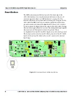
LED Indicators

LED indicators show power on, sampling rate, lock to an external 
sampling reference, and external sampling reference source errors.

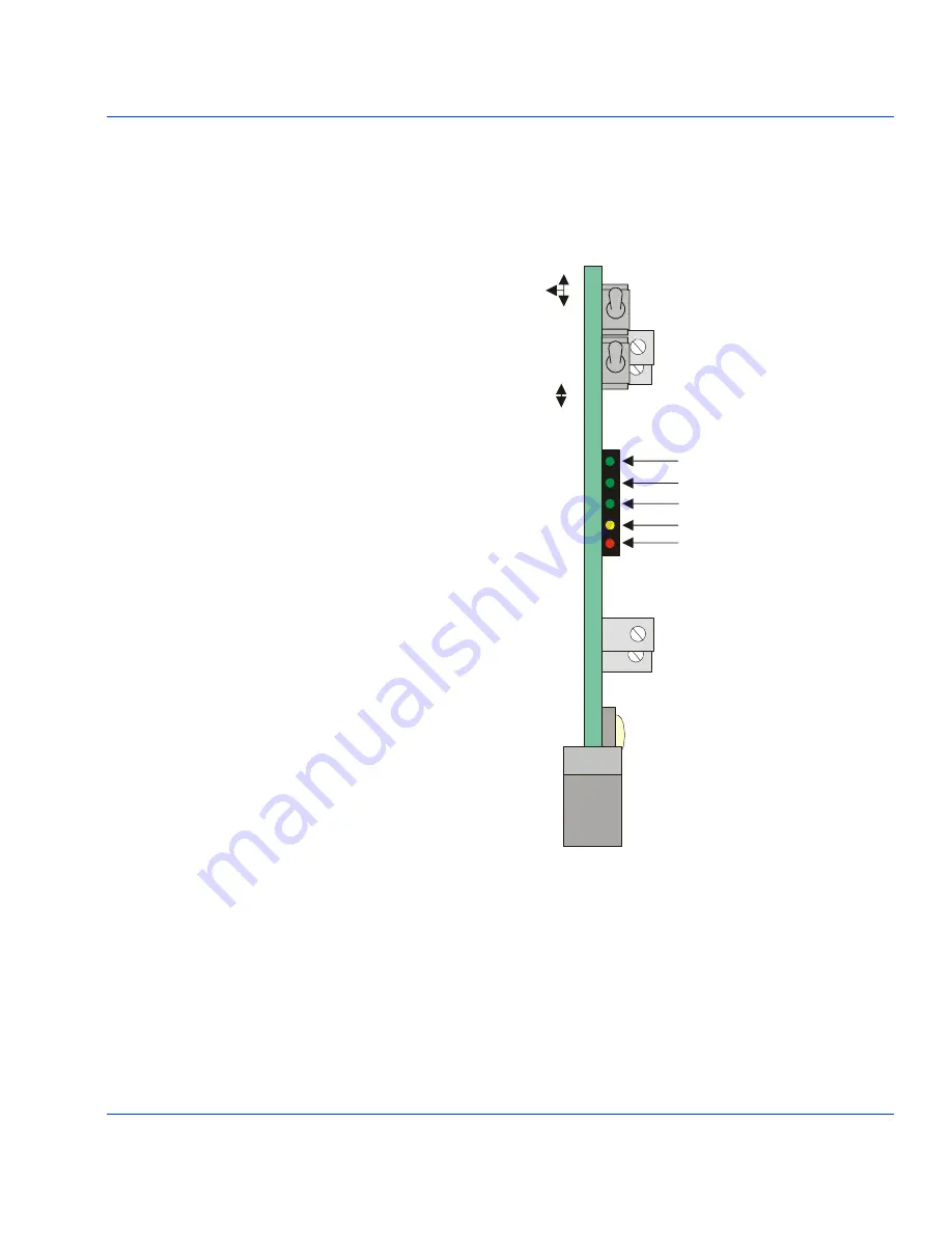
Figure 2-6. 

Card-Edge View

Power LED

The green power LED indicates that voltage is present across the +V and 
-V inputs to the ADC-6880. It does not guarantee that the input power is 
within the proper ± 6.5 to ± 8.0 V input voltage range. It also does not 
indicate that each of the voltage regulators is working properly.

R15
R21

SW3

SW2

AUTO

INT

EXT

48 kHz

44.1 kHz

Gain Adjust

Right Channel

Green LED

Red LED

Yellow LED

Green LED

Green LED

PWR

REF ERR

EXT REF

44.1 kHz

48 kHz

Gain Adjust

Left Channel

R125

R113

SW1

Reset

Button

Summary of Contents for 6800/7000 Series

Page 1: ...6800 7000 Series Audio and Video Multi Demultiplexing Products Installation and Operation Manual 175 000061 00 Edition B ...

Page 2: ...S LogoMAX LogoMotion Media File MediaPort MIX BOX Monarch Motion File NEO OPUS PanelMAPPER Pilot Portal PROM Slide RouterWORKS StillFile Still Net Tekniche Unilock VIA ViewGuard Xplus and Leitch XPRESS are trademarks or registered trademarks of Leitch Technology Corporation in the United States Canada and or other countries All other trademarks are the property of their respective owners Copyright...

Page 3: ...6800 7000 Series Audio and Video Multi Demultiplexing Products Installation and Operation Manual Edition B November 2002 ...

Page 4: ......

Page 5: ...your understanding the authors of this manual have adhered to the following text conventions Bold Indicates dialog box property sheet field button checkbox listbox combo box menu submenu window list and selection names Italics Indicates email addresses names of books and publications and first instances of new terms and specialized words that need emphasis CAPS Indicates a specific key on the keyb...

Page 6: ...and Video Multi Demultiplexing Products Installation and Operation Manual Revision History Edition Date Revision History A May 1998 Initial release B November 2002 Updated information General reformatting and reorganization of material ...

Page 7: ...onizer Module Chapter 7 DEC 6804 Decoder and DES 6804 Decoder with Frame Synchronizer Chapter 8 ENC ENS ENX 6801A Encoder Modules Chapter 9 MXA 6800 AES and MXA 6801 A2 A4 Audio Multiplexer Module Chapter10 VFS 6801 Serial Component Frame Synchronizer Module Chapter 11 VTS 6801 Video Timing Switcher Appendix A Embedding Modes Graphic Description Test Series Manual Chapter 1 VTG 6801 1 VTG 6801 1A ...

Page 8: ...VEA 6840 Video Equalizing Amplifier Module Chapter 8 VPD 6830 Programmable Video DA series Chapter 9 VSD 6801 Serial Digital Distribution Amplifier Module Chapter 10 VSE 6801 Serial Equalizing Amplifier Module Chapter 11 VSE 6802 Serial Equalizing Distribution Amplifier Chapter 12 VSM 6802 Digital Composite Video Signal Chapter 13 VSM 6804 Digital Composite Video Signal Monitor Module Chapter 14 V...

Page 9: ...1 Mounting Frames Chapter 2 FR 6801 FR 6801 1 Frames Chapter 3 FR 6804 FR 6804 1 Frames Chapter 4 CF 6801 Cooling Frame Chapter 5 FR 7001 and FR 7000MB MIXBOX Chapter 6 6801PS Power Supply Module Chapter 7 6804 1 Power Supply Module Chapter 8 7000 Power Supply Module Chapter 9 6801PS 48 Power Supply Module Chapter 10 6804PS 1 48 Power Supply Module ...

Page 10: ...our own packaging as long as it meets the following criteria Packaging must be able to withstand the product weight Product must be held rigid within the packaging There must be at least 2 inches of space between the product and the container The corners of the product must be protected Products that are being returned to Leitch for servicing should be shipped prepaid in the original packaging mat...

Page 11: ...operate normally or has been dropped Safety Terms and Symbols Terms and Symbols in This Manual Terms and Symbols on the Product WARNING Statements identifying conditions or practices that can result in personal injury or loss of life High voltage is present Uninsulated dangerous voltage within the product s enclosure may be sufficient to constitute a risk of electric shock to persons CAUTION State...

Page 12: ...NG Potentially lethal voltages are present within this product s frame during normal operation The AC power cord must be disconnected from the frame before the top panel is removed In frames with multiple power supplies remove ALL power cords Power should not be applied to the frame while the top is open unless properly trained personnel are servicing the unit PL Poland Przod zdjeciem pokrywy wyci...

Page 13: ...6800 7000 Series Audio and Video Multi Demultiplexing Products Installation and Operation Manual xi Preface AVIS Risque de choc electrique Ne pas ouvrir ...

Page 14: ...t United Kingdom WARNING THIS APPLIANCE MUST BE EARTHED Sweden APPARATEN SKALL ANSLUTAS TILL JORDAT UTTAG NÄR DEN ANSLUTS TILL ETT NÄTVERK Do Not Operate Without Covers To avoid electrical shock or fire hazard do not operate this product with covers or panels removed Use Proper Fuse To avoid fire hazard use only the fuse type and rating specified for this product Do Not Operate in Wet Damp Conditi...

Page 15: ...fied by the Manufacturer Do Not Operate With Suspected Failures Refer all servicing to qualified service personnel Servicing is required when the apparatus has been damaged in any way such as power supply cord or plug is damaged liquid has been spilled or objects have fallen into the apparatus the apparatus has been exposed to rain or moisture does not operate normally or has been dropped For Prod...

Page 16: ...us including amplifiers that produce heat Install Near Socket Outlet The equipment shall be installed near the socket outlet and a disconnect device shall be easily accessible Protect the Power Cord Protect the power cord from being walked on or pinched particularly at plugs convenience receptacles and the point where they exit from the apparatus Attention Observe precautions for handling electros...

Page 17: ...oi rajahtaa jos se on virheellisesti asennettu Vaihda paristo ainoastaan valmistajan suosittelemaan tyyppun Havita kaytetty paristo valmistajan ohjeiden mukaisesti SE Sweden VARNING Explosionsfara vid felaktigt batteribyte Anvand samma batterityp eller en eller en ekvivalent typ som rekommenderas av tillverkaren Kassera anvant batteri enligt fabrikantens instruktion D Denmark KO Korean Advarsel Li...

Page 18: ...stalling or removing sensitive components Use a Safe Work Area Do not use any devices capable of generating or holding a static charge in the work area where you install or remove sensitive components Avoid handling sensitive components in areas that have a floor or benchtop surface capable of generating a static charge Handle Components Carefully Do not slide sensitive components over any surface...

Page 19: ...ng control apparatus for professional use Part 1 Emission Environment E4 EN55103 2 Electromagnetic compatibility Product family standard for audio video audio visual and entertainment lighting control apparatus for professional use Part 2 Emission Environment E4 EN61000 4 2 Electrostatic discharge requirements ESD 2kV CD 4kV AD EN61000 4 3 Radiated radio frequency electromagnetic field immunity te...

Page 20: ...tus ICES 003 of the Canadian Department of Communications Safety Standards Safety Standards 6801PS 48 Only EN60065 Safety requirements for mains operated electronic and related apparatus for household and similar general use IEC 60065 1985 5th Edition A1 1987 A2 1989 A3 1992 modified per the provision of the Low Voltage Directive 73 23 EEC of February 19 1973 as amended by 93 68 EEC UL 1419 Safety...

Page 21: ...mation technology equipment including electrical business equipment IEC 60950 1999 per the provision of the Low Voltage Directive 73 23 EEC of February 19 1973 as amended by 93 68 EEC UL 1950 Safety of information technology equipment including electrical business equipment CSA C22 2 No 950 Safety of information technology equipment including electrical business equipment ...

Page 22: ...Preface xx 6800 7000 Series Audio and Video Multi Demultiplexing Products Installation and Operation Manual ...

Page 23: ...tering as per CCIR 601 Specifications 4 Frequency Response 4 Signal to Noise Ratio 4 Output 4 Installation 5 Module Edge Layout 6 Setup and Control 8 Front Edge Controls 8 Jumpers 10 Standard Select Function 11 Analog Adjustments 14 Sync Phase 14 Cb Gain and Cr Gain 14 Cb Phase and Cr Phase 14 Chapter 2 ADC 6880 Analog to AES EBU Digital Audio Converter 15 Overview 15 Operation 17 Analog Audio Inp...

Page 24: ...alog Audio Input 27 Reference Input 27 Digital Output 27 Performance Specifications 28 Power Specifications 28 ADC 6880 29 Implementation Chart 29 Chapter 3 ADM ASM 680x Embedded Audio Monitoring Serial Distribution Amplifier Modules 31 Overview 31 Frames and Modules 32 Serial Video Input 34 Serial Video Outputs ASM 6800 only 34 Analog Audio Outputs 35 Balanced Audio Outputs 36 Module Edge Control...

Page 25: ...ol 52 Switches 54 Color Bar Levels 55 Analog Adjustments 57 Specifications 58 Serial Video Input 58 Component Outputs 58 Sync Outputs 59 Power Consumption 59 Chapter 5 DAC 6880 AES EBU Digital Audio to Analog Audio Converter 61 Overview 61 Operation 63 Input Impedance 63 Terminated or Looping Inputs 63 Full Scale Analog Output Level 63 Output Level Adjustment 64 Power and Error Indicators 64 Rear ...

Page 26: ...hasing 71 Storage 71 Reference Input 71 Power Dissipation 72 Installation 73 Operations 74 Controls 74 LED Indicators 74 Jumpers 75 Switches 75 Frame ID 75 Bank A1 76 Bank B2 78 Chapter 7 DEC 6804 Decoder and DES 6804 Decoder with Frame Synchronizer 79 Overview 79 Features 80 Signal Flow 81 Front and Back Modules 82 Front Module 82 Back Module and Adhesive Overlay 83 Installation 85 Jumper Setting...

Page 27: ...4 Storage DES 6804 104 Audio Synchronization Interface Output DES 6804 104 Reference Input DES 6804 104 Module Start Up 105 Typical Power Dissipation 105 Chapter 8 ENC ENS ENX 6801 M Encoder Modules and Accessories 107 Overview 107 Features 108 Specifications 109 Serial Video Inputs 109 Video Outputs 109 Phasing Range 111 Power Consumption 111 Reference Inputs 111 Installation 113 Block Diagram 11...

Page 28: ...io 128 MXA 6800 AES 128 MXA 6801 A2 A4 128 Terminology 129 Installation 130 Jumper Settings 135 MXA 6800 AES 136 MXA 6800 A2 A4 137 Operation 137 Common Mode Adjust Potentiometers pots 138 LED Indicators MXA 6800 AES 138 LED Indicators MXA 6801 A2 A4 140 Toggle Switch and LED Display Operation 141 Control Parameters Summary 142 Operator Mode 1 OS1 143 Operator Mode 2 OS2 145 Operator Mode 3 OS3 14...

Page 29: ...apter 10 VFS 6801 Serial Component Frame Synchronizer Module 163 Overview 163 Specifications 164 Serial Video Inputs 164 Serial Video Outputs 164 Phasing 165 Storage 165 Reference Input 165 Installation 166 Operations 167 Controls 167 LED Indicators 167 Jumpers 167 Switches 168 Chapter 11 VTS 6801 Video Timing Switcher 171 Overview 171 Features 172 Specifications 173 Serial Video Inputs 173 Serial...

Page 30: ...GPI Controls 185 Polarity Active High 185 Polarity Active Low 185 General Issues 186 Applications 187 Clean Switch Settings 187 2 by 1 Clean Switch Settings 187 Digital Adjusted Line Delay 188 Backup Video Switch 189 Appendix A Embedding Modes Graphic Description 191 Overview 191 Left Mode Justify 192 Follow Mode Part 1 193 Follow Mode Part 2 194 Overwrite Mode Part 1 195 Overwrite Mode Part 2 196...

Page 31: ...omponent analog to digital 4 2 2 conversion It provides ten bit or optionally eight bit conversions from 525 and 625 line analog component signals to SMPTE 259 C serial digital video The ADC 6801 supports the following standards SMPTE EBU GBR and YPbPr NTSC related GBR MII related GBR and YPbPr BETACAM YPbPr in 625 and 525 line standards with and without setup as appropriate Specifications and des...

Page 32: ... 8 bit conversion Component analog input with color space conversion GBR or YPbPr Looping inputs Two serial digital SMPTE 259 C 270 Mb s outputs Selectable sync from Y G external color black or TTL level Digital filtering as per CCIR 601 specifications 12 dB at Nyquist 2x oversampling Variable vertical blanking up to line 19 for 525 and line 22 for 625 EDH insertion Horizontal blanking markers for...

Page 33: ...27 MHz Y 13 5 MHz Cr Cb Quantization 10 bits Input Standards SMPTE EBU MII Betacam component or RGB at 525 or 625 line rates External sync and G Y B B Y R R Y loop through 5 BNCs Ext Sync Loop through G Y B B Y R R Y Item Specifications Connector BNC per IEC 169 8 Impedance Loop through high impedance or 75Ω Signal Level 1 Vp p nominal with sync 0 7 Vp p nominal Adjustable Gain 10 Time Adjustment ...

Page 34: ...put Item Specifications Y Channel 0 1 dB to 5 5 MHz Cr Cb Channels 0 2 dB to 2 75 MHz Item Specifications On all Channels 64 dB RMS relative to 0 714 V 10 kHz to 5 5 MHz Interchannel Crosstalk 50 dB 2T K Factor 0 5 Luminance Non linearity 1 Gain Alignment 1 typically better than 0 5 DC Clamping Typically within 1 quantization level on field average Item Specifications Output Standard 4 2 2 two BNC...

Page 35: ...ternal sync input can be terminated on board by installing jumper J8 or can be externally looped See Figure 1 2 on page 7 and see also Setup and Control on page 8 for further information Signal Descriptions Sync In External color black or TTL level sync optional G Y Green or Y signal looped B B Y Blue or B Y signal looped R R Y Red or R Y signal looped Serial Out SMPTE 259 C serial outputs ADC 680...

Page 36: ...lation and Operation Manual Module Edge Layout The table below describes the SW1 Hex switch positions and functions Position Function 0 Operate 1 Standard Select 2 YCrCb Gain 3 Cb Gain 4 Cr Gain 5 Y Offset 6 Cb Offset 7 Cr Offset 8 H Phase 9 Luma Phase A Split Screen B Markers C Color Bars D Vertical Blanking E Factory Recall F Reserved ...

Page 37: ...dule Figure 1 2 Front Edge Layout and Controls TOG SW2 LEDs HEX SW1 ADC 6801 525 AUTO 625 LOCK SMPTE BETA M II NTSC GBR Y Pr Pb SETUP SYNC G Y SYNC TTL SYNC BLK 8BIT MODE ACTIVITY J6 OP CAL J7 OP CAL Config Error J5 OP CAL J8 HI Z 75 U4 System Firmware Sync Phase CR Phase CB Phase CB Gain CR Gain J5 J6 and J7 must be in OP position for correct board operation ...

Page 38: ...DN No Action 1 Standard Select Standard selection is achieved by setting the HEX switch in position 1 Toggling SW2 up moves the selection through all of the modes Toggling SW2 down changes the selection inside of the mode The Active mode selection is indicated by the current selection LED flashing UP DN Change Mode Change Selection 2 YCrCb Gain Changes the overall gain on all three channels at the...

Page 39: ...P DN Increase Gain Decrease Gain 8 Horizontal Phase Changes the timing adjustmentsbetweenthe input video and the sync reference The adjustmentismade in27 MHz 37 ns increments or decrements UP DN Increase Gain Decrease Gain 9 Luma Phase Adjusts the 13 5 MHz cycle time delay between Y and the Cb Cr channels UP DN Increase Gain Decrease Gain A Split Screen Enables a vertical split between the input s...

Page 40: ...nd 75 chroma 100 0 75 0 UP DN Enabled Disabled D Vertical Blanking Varies the blanking width up to line 19 in 525 and line 22 in 625 standard UP DN Increase Gain Decrease Gain E Factory Recall Recalls the factory auto calibrated levels for the given input This recall resets all of the user offsets to zero and restores the factory Luma and Horizontal phases See Factory Recall Standards on page 11fo...

Page 41: ...de Selections Purpose Standard 525 Auto 625 Selects 525 line or 625 line input The Auto position will automatically determine the input line standard and set the system accordingly Format SMPTE BETA MII NTSC Selects the input format SMPTE BETA MII or NTSC Matrix selects the input matrix GBR or YPbPr Matrix GBR YPbPr Selects the input matrix GBR or YPbPr Setup On off Setup consists of On Off contro...

Page 42: ...d 525 GBR with No Setup G B R SMPTE 700 mV 700 mV 700 mV BETA Invalid MII 700 mV 700 mV 700 mV NTSC 714 mV 714 mV 714 mV 525 GBR with Setup G B R SMPTE Invalid BETA Invalid MII related 700 mVp p 648 mV 52 mVsetup 700 mVp p 648 mV 52 mV setup 700 mVp p 648 mV 52 mVsetup Illegal standards can be selected indicated by flashing Activity LED In this situation the system software will choose the closest...

Page 43: ...AV to SDI Converter Module 525 GBR with Setup G B R NTSC related 714 mVp p 660 mV 54 mVsetup 714mVp p 660mV 54mV setup 714mVp p 660mV 54mVsetup 625 YPbPr Y B Y R Y EBU 700 mV 700 mV 700 mV BETA non EBU 700 mV 934 mV 934 mV MII related Invalid NTSC related Invalid 625 GBR G B R EBU 700 mV 700 mV 700 mV BETA Invalid MII Invalid NTSC Invalid ...

Page 44: ...ects fine phasing to the system sync signal within one 27 MHz cycle or 37 ns Cb Gain and Cr Gain Used to null the gain errors between the GBR to YPbPr analog matrix They are set in the factory and there should be no need to adjust them Cb Phase and Cr Phase Selects fine phasing of the CB and CR channels to the Y channel within 5 ns These are set in the factory and there is no need to readjust them...

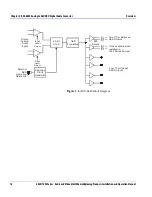
Page 45: ...75Ω unbalanced digital outputs when used in the 6800 series frame or 75Ω unbalanced and 110Ω balanced digital outputs when used in a 7000 series frame The ADC 6880 utilizes a 20 bit 64X oversampling Sigma Delta A to D converter that can sample the audio signal at 48 kHz or 44 1 kHz based on an external reference signal or on an internal reference signal generated on board The audio signal may also...

Page 46: ...llation andOperation Manual Figure 2 1 ADC 6880 Block Diagram Two 110 Balanced AES Outputs Only available when installed in 7000 Series frames Ω Four 75 Coaxial AES Outputs Ω Stereo Analog Audio Inputs External AES Sampling Reference Input Level Adjust Input Level Adjust 485 Drivers AES Formatting 20 bit A to D Sampling Clock Generator ...

Page 47: ...he gain adjustments are set at the factory from a high precision audio test reference signal such that the full scale digital output level 0 dBFS corresponds precisely with the calibrated selectable attenuator positions of 16 dBu to 30 dBu described above The gain can be adjusted by the user to match specific level requirements for full scale digital audio signal levels In addition to performing a...

Page 48: ...its to be synchronized to a common AES11 sampling reference signal such as that generated from the Leitch DAR 6880 reference generator A standard AES3 digital audio signal may also be used The ADC 6880 cannot accept word clock or a video signal as a reference input The ADC 6880 can be locked to a video signal through the use of Leitch s DAR 6880 reference generator which can be locked to video See...

Page 49: ...t over a 14 dB range from 16 dBu analog input 0 dBFS digital output to 30 dBu analog input 0 dBFS digital output in calibrated 2 dB increments This range of input levels allows operators to set the ADC 6880 such that the full scale digital output 0 dBFS will match their maximum analog audio signal level Because the attenuation network is of sufficient precision the gain potentiometers do not have ...

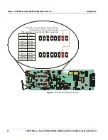
Page 50: ...oducts Installation andOperation Manual Figure 2 2 Attenuation Jumper Settings ADC 6880 Jumpers Level J1 J12 J2 J13 J3 J14 J4 J15 J6 J17 J5 J16 J7 J18 J8 J19 16 dBu 18 dBu 20 dBu 22 dBu 26 dBu 24 dBu 28 dBu 30 dBu To set the required level apply jumpers to the proper set of jumper prongs This example shows that 28 dBu is selected ...

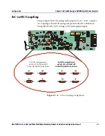
Page 51: ...udio input to be AC or DC coupled AC coupling is the default setting and prevents the ADC 6880 from being disturbed by a DC voltage on the analog input signal Figure 2 3 AC or DC Coupling Configuration ADC 6880 For DC coupled input set J9 J10 J20 and J21 to the DC position as shown For AC coupled input set J9 J10 J20 and J21 to the AC position as shown For DC coupled input set J9 J10 J20 and J21 t...

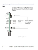
Page 52: ...ignal level to be matched to a known analog input level from a test generator Figure 2 4 Card Edge View R15 and R113 are multi turn potentiometers used to adjust gain R21 and R125 are multi turn potentiometers used to adjust common mode rejection These are factory set and adjustment is not normally required R15 R21 SW3 SW2 AUTO INT EXT 48 kHz 44 1 kHz Gain Adjust Right Channel Green LED Red LED Ye...

Page 53: ...eference signal present on the external reference input If no signal is present or if the signal becomes unusable the ADC 6880 will automatically switch to internal Reference mode When the external reference signal is present and usable the ADC 6880 will automatically switch back to external Sampling mode and will be locked to the external reference signal The external setting forces the ADC 6880 ...

Page 54: ...so mutes the digital data at the output of the ADC 6880 During this reset time approximately 1 second the analog audio input signal is disconnected and the inputs are shorted to ground This is accomplished via relays RL1 and RL2 Inputs are not shorted to ground The reset procedure removes any DC offsets present on the ADC 6880 input circuit and any DC offset in the A to D converter IC s internal i...

Page 55: ... Figure 2 6 Card Edge View Power LED The green power LED indicates that voltage is present across the V and V inputs to the ADC 6880 It does not guarantee that the input power is within the proper 6 5 to 8 0 V input voltage range It also does not indicate that each of the voltage regulators is working properly R15 R21 SW3 SW2 AUTO INT EXT 48 kHz 44 1 kHz Gain Adjust Right Channel Green LED Red LED...

Page 56: ...via the Ref Pres LED but will not have either sampling frequency LED illuminated This condition is valid but the external reference signal must be between 32 and 50 kHz for the A to D converter IC to be able to lock to it External Reference Present The yellow Ext Ref LED indicates that an external reference is present the ADC 6880 is locked to it and using it as the sampling reference If the ADC 6...

Page 57: ...Ω Maximum Input Level 30 dBu Input Level Settings 16 dBu to 30 dBu 0 dBFS in 2 0 dB increments jumper selectable 2 0 dB variable adjustment range Item Specifications Reference Signal Type AES11 or AES3 audio reference signal Input Type BNC loop through Input Impedance 10 kΩ Item Specifications Number of Outputs in 6800 Series Frame 4 Outputs 75Ω BNC Number of Outputs in 7000 Series Frame 2 Outputs...

Page 58: ...Specifications Power Specifications Item Specifications Frequency Response 0 05 dB 20 Hz to 20 kHz Linearity 1 0 dB to 100 dBFS Signal to Noise Ratio 107 dB 20 Hz to 20 kHz A weighted 102 dB 20 Hz to 20 kHz unweighted THD N 95 dB 20 Hz to 20 kHz 2 dBFS Item Specifications Consumption 3 5 W at 6 8 VDC Input Voltage 6 4 to 7 5 VDC Current 160 mA on 6 8 VDC rail 350 mA on 6 8 VDC rail ...

Page 59: ... Nonaudio N N Y N 2 4 Emphasis 000 Not indicated 100 No emphasis 110 50 15 µs 111 CCITT J17 N N N N N Y N N 5 0 Fs locked 1 Fs unlocked Y Y Y Y 6 7 00 Not indicated 01 48 KHz 10 44 1 KHz 11 32 KHz N Y Y Y N Y Y Y 1 0 3 Channel mode 0000 Not indicated 0001 2 channel 0010 Mono 0011 Primary secondary 0100 Stereo 0101 to 1111 N N N N N N N N N N Y N 4 7 User bit mode 0000 Not indicated 0001 192 bit 00...

Page 60: ...s N N N Y N N 3 0 7 Multichannel modes N N 4 0 1 AES11 sync reference N N 5 0 7 Unused N N 6 9 ASCII source ID N N 10 13 ASCII destination ID N N 14 17 Local sample address N N 18 21 Time of day address N N 22 0 7 C data reliability N N 23 0 7 CRCC N Y Validity V bit N Y User U bit N Y Audio sampling frequencies KHz 32 44 1 48 RX 48 TX Audio sample word length bit 16 24 bit RX 20 bit TX Byte Bit F...

Page 61: ...he need for low cost monitoring of audio signals that are embedded within the serial video signal The ASM provides analog audio outputs while the ADM has both analog and digital AES output capability To view the number and types of outputs provided by each module when mounted in either the FR 680x or FR 7001 series mounting frames See Mounting Frames and Modules on page 32 Specifications and desig...

Page 62: ...channels The ADM 6804 provides two or four analog audio outputs and two balanced digital audio channel outputs depending upon the mounting frame used The ADM 6800C provides four reclocked serial digital video outputs and two single ended AES channels each with two outputs The ADM 6804BC used only in the FR 680x series mounting frames has two balanced AES output channels and two single ended AES ch...

Page 63: ...with two outputs and two analog audio outputs The ADM 6804BC 70 and 68 has two single ended AES channels each with two outputs and two or four analog audio outputs depending on the mounting frame All modules accept composite 143Mb s or component 270Mb s 525 or 625 line video with audio multiplexed into the ancillary data area according to SMPTE 272M The operating mode incoming serial video data ra...

Page 64: ...embedding Connector BNC per IEC 169 8 Impedance 75Ω Return Loss 18 dB to clock frequency Signal Level 800 mV 10 Common Mode Rejection 30 Vp p up to 60 Hz Equalization Automatic up to 21 dB for 143 Mb s 23 dB for 270 Mb s Item Specifications Number of Outputs 4 Standards SMPTE 259M A 143 Mb s 525 NTSC 272M AB audio embedding 259M C 270 Mb s 525 625 component Connector BNC per IEC 169 8 Impedance 75...

Page 65: ...ical Signal to Noise 90 dB 50 20kHz E Inter channel Crosstalk 90 dB 50 20kHz Frequency Response full scale output 50 Hz 10 kHz 0 0 15 dB 10 kHz 20 kHz 0 0 3 dB Power Requirement ASM 68xx Positive rail 4 3 W Negative rail 0 70 W Total 5 0 W Power Requirement ADM 68xx Positive rail 4 5 W Negative rail 2 9 W Total 7 4 W Single ended Digital Audio Outputs Number of outputs Number of outputs 2 outputs ...

Page 66: ...allation and Operation Manual Balanced Audio Outputs Figure 3 1 ADM Series Modules Item Specifications Number of Outputs 1 output at 1 or 2 AES channels Standards AES 3 1992 ANSI 54 40 1992 Impedance 110Ω 1 2 3 4 VID_PRES AUD_PRES AUD_ERR NO_LOCK MAIN SWAP MONITOR REMOTE SWAP DEMUX DACS AUDIO GROUP SELECT AES ENCODER DRIVERS SERIAL VIDEO AES OUTPUTS ANALOG OUTPUTS 1A 1B 2A 2B ...

Page 67: ...ach group may be comprised of a maximum of two digital audio channels in the AES format In turn each AES channel is composed of two monaural audio channels Thus one audio group may contain up to four monaural audio channels For purposes of this manual the main AES channels are designated as 1 and 2 and the sub channels as A and B Therefore an audio group can be thought of as containing channels 1A...

Page 68: ...y analog outputs making the main and monitor swaps redundant The user can use either swap to perform the appropriate routing to outputs The intention of main swap control is to allow the user to appropriately set the routing of particular audio channels to the specific output connectors The main swap control affects both analog and digital outputs SW1 enables a swap between channel pairs 1 and 2 S...

Page 69: ...ported when the module is installed in an FR 7001 frame External contact closures are provided for this feature This feature is enabled by appropriately setting the Swap Control mode Jumper J3 See Figure Jumper Configurations on page 44 and Figure 3 6 ADM ASM 680X PCB Jumper and Switch Locations on page 46 Analog Output Levels Peak analog audio levels are user adjustable and accessible pots are pr...

Page 70: ...e Indicator Descriptions The ASM ADM series modules have the following module edge indicators Audio Group DIP SW3 DIP SW4 Group 1 Down Down Group 2 Up Up Group 3 Down Down Group 4 Up Up For 143 Mb s serial video applications Group 1 must be selected LED Indicator Function VID_PRES Indicates the presence of a valid video present or input AUD_PRES Indicates the presence of a selected embedded audio ...

Page 71: ...ASM 6800 Module ASM 6800 M ADM 6800 M CH2 AES CH1 CH1 A B 1 2 A B A B SERIAL OUTPUTS SERIAL OUTPUTS INPUT INPUT REMOTE REMOTE A B A B 1 2 1 2 1 1 2 2 3 3 4 4 ANALOG ADM 6804BC M CH2 CH1 A B A B ANALOG OUTPUTS UNBALANCED AES OUTPUTS 1 2 1 2 REMOTE SERIAL INPUT A B 1 2 ADM 6804 M ADM 6800C M CH2 CH1 A B A B INPUT REMOTE A B 1 2 ANALOG OUTPUTS AES OUTPUTS 1 2 UNBALANCED AES OUTPUTS SERIAL OUTPUTS SER...

Page 72: ...rresponding overlay is placed on the rear panel Figure 3 4 ADM ASM Module ASM 6800 SERIAL INPUT SERIAL OUTPUT ANALOG AUDIO OUTPUT 1 2 3 4 1B 1B 1A 1A ADM 6800 SERIAL INPUT SERIAL OUTPUT AES OUTPUTS 1 2 3 4 2 2 1 1 ASM 6804 SERIAL INPUT 1B 1B 1A 1A 2B 2B 2A 2A ANALOG AUDIO OUTPUT ADM 6804 SERIAL INPUT AES OUTPUTS 1B 1B 1A 1A 2 2 1 1 ANALOG AUDIO OUTPUT SERIAL INPUT SERIAL INPUT BALANCED AES OUTPUTS...

Page 73: ...pters The 6800AA 6800AD 6800B AA 6800B AD and 6804BC AA are audio adapters that can be placed on top of the overlay and plugged into the BNCs of the FR 680x series frame for different output formats Figure 3 5 Audio Adapters 6800 AA A LEFT A LEFT B RIGHT B RIGHT CHANNEL 1 CHANNEL 2 6800 AD A LEFT 1 B RIGHT 2 ANALOG OUTPUTS AES OUTPUTS 6800B AA A B ANALOG OUTPUTS 6804BC AA A B ANALOG OUTPUTS 6800BC...

Page 74: ...0X 6800B AD Rear connector adapter required J31 J32 J33 J34 on DIG side ADM 6800 70 FR 7001 ADM6800 M Rear connector adapter required J11 J12 J13 J14 on DIG side J31 J32 J33 J34 on DIG side ADM 6800 C FR 680X No rear connector adapter required J31 J32 J33 J34 on DIG side ADM 6800 C 70 FR 7001 ADM 6800 M Rear connector adapter required J31 J32 J33 J34 on DIG side ADM 6804 68 FR 680X 6800 AD Rear co...

Page 75: ...Rear connector adapter required J31 J32 J33 J34 on DIG side ASM 6800 70 FR 7001 ASM 6800 M Rear connector adapter required J11 J12 J13 J14 on AN side J31 J32 J33 J34 on AN side ASM 6804 FR 7001 6800AA Rear connector adapter required J21 J22 J23 J24 on AN side J31 J32 J33 J34 on AN side Jumper Positions within a Jumper Block component side top view Type Mounting Frame Required Back Box and Jumper S...

Page 76: ... Audio Monitoring Serial Distribution Amplifier Modules Jumper Configurations 46 6800 7000 Series Audio and Video Multi Demultiplexing Products Installation and Operation Manual Figure 3 6 ADM ASM 680X PCB Jumper and Switch Locations ...

Page 77: ...g Component Converter addresses the requirements of broadcasters and video professionals for component digital to analog 4 2 2 conversion The DAC 6801 supports the following standards in 625 and 525 line standards with and without setup as appropriate SMPTE EBU GBR and YPbPr NTSC related GBR MII related GBR and YPbPr BETACAM YPbPr Specifications and designs are subject to change without notice ...

Page 78: ...c output Dual outputs Serial digital SMPTE 259M C 270 Mb s input Selectable sync on GBR 4x oversampling Y 8x oversampling PbPr Variable vertical blanking up to line 20 for 525 and line 22 for 625 Low power 6 5 W Color bar generator See Figure 4 7 for a functional block diagram of the DAC 6801 Figure 4 7 DAC 6801 Functional Block Diagram Program In Sync out 3V Y G Out B Pb Out Y Pr Out Auto EQ Flag...

Page 79: ...re 4 8 DAC 6801 Back Module Connectors Front Edge Layout The DAC 6801 front edge layout is shown in the following figure The two switches on the front are used for setup and control Hex SW1 has 16 positions Hex 0 to F SW2 is a toggle type switch Press up or down to toggle See Figure 4 9 on page 50 Signal Description Serial In SMPTE 259 C Serial Inputs G Y Green or Y signal B B Y Blue or B Y signal...

Page 80: ...525 Indicates the module is running in 525 line mode AUTO Indicates the module is running in AUTO mode the line mode is automatically changed as per the input signal 625 Indicates the module is running in 625 line mode LOCK Indicates the module is locked to the input serial video ERROR Indicates the module has detected EDH errors in the input serial video SMPTE BETA M 11 NTSC Indicates the current...

Page 81: ...or offset has been modified from factory settings with SW1 in Position 0 This LED illuminates as SW1 is rotated in positions 2 through 7 indicating which parameter has been adjusted for gain and offset The Detent LED blinks when an invalid standard has been selected for example 625 NTSC ACTIVITY Indicates calibration activity used only during alignment LEDs Function Config Error J8 HI Z 75 J6 HI Z...

Page 82: ...following steps to make a selection 1 Set HEX SW1 to position 1 2 Toggle SW2 Up to move through all of the Operating modes The corresponding LED illuminates as the selection is toggled 3 Toggle SW2 Down to change the selection inside the mode The corresponding LED illuminates as the selection is toggled UP DN Change Mode Change Selection 2 GBR YPrPb Gain Allows the operator to change the overall g...

Page 83: ... The range is from a minimum of 5 µs to one line length delay UP DN Increase Delay Decrease Delay 9 Not Used Not Used Not Used A Not Used Not Used Not Used B Not Used Not Used Not Used C Internal Color Bars Enables the Color Bars signal The bars are 100 luma and 75 chroma 100 0 75 0 The specified level for each standard refers to 100 color bar levels 100 0 100 0 100 7 100 0 or 100 7 5 100 7 5 for ...

Page 84: ...ly determine the input line standard and set the system accordingly Format SMPTE BETA MII or NTSC Allows the user to select the input format Matrix GBR or YPbPr Allows the user to select the input matrix Setup On Off An On Off control based on the input standard On Off enabled the setup is added to the analog signal in the digital domain Sync Source C Y BLK TTL Sync source selects are as follows I...

Page 85: ...olor Bar Levels 525 YPbPr with Setup Y PB Pr SMPTE 700 mV 700 mV 700 mV BETA 714 mV 1008 mV 1008 mV MII 700 mV 648 mV 648 mV NTSC Invalid SMPTE Invalid BETA 714 mVp p 660 mV 54 mV setup 934 mV 934 mV MII 700 mVp p 648 mV 52 mV setup 648 mV 648 mV NTSC Invalid 525 GBR with No Setup G B R SMPTE 700 mV 700 mV 700 mV BETA Invalid MII 700 mV 700 mV 700 mV NTSC 714 mV 714 mV 714 mV ...

Page 86: ... 52 mV setup 700 mVp p 648 mV 52 mV setup 700 mVp p 648 mV 52 mV setup NTSC related 714 mVp p 660 mV 54 mV setup 714 mVp p 660 mV 54 mV setup 714 mVp p 660 mV 54 mV setup 625 YPbPr Y PB Pr EBU 700 mV 700 mV 700 mV BETA non EBU 700 mV 934 mV 934 mV MII related Invalid NTSC related Invalid 625 GBR G B R EBU 700 mV 700 mV 700 mV BETA Invalid Invalid Invalid MII related Invalid Invalid Invalid NTSC re...

Page 87: ...tion and Operation Manual 57 Analog Adjustments Chapter 4 DAC 6801 Digital to Analog Component Converter Analog Adjustments Pb Phase and Pr Phase allow fine phasing of the Pb and Pr channels to the Y channel within 5 ns They are set in the factory and do not need adjusting ...

Page 88: ...rn Loss 18 dB to clock frequency Common Mode Rejection 30 Vp p up to 60 Hz Equalization Automatic up to 22 dB Item Specifications Number of Outputs 6 BNCs 2 sets of G Y B B Y R R Y Output Standards SMPTE Betacam MII NTSC Y B Y R Y or GBR where applicable Impedance 75Ω Return Loss 36 dB to 5 MHz on all outputs Quantizing 10 bits Gain Adjustable Range 30 DC Adjustable Offset 5 mV Frequency Response ...

Page 89: ... Products Installation and Operation Manual 59 Specifications Chapter 4 DAC 6801 Digital to Analog Component Converter Sync Outputs Power Consumption Item Specifications Number of Outputs 2 Output Level 0 3 Vp p Item Specifications 6 5 W 6 5 1A 6 5 35 mA ...

Page 90: ...Chapter 4 DAC 6801 Digital to Analog Component Converter Specifications 60 6800 7000 Series Audio and Video Multi Demultiplexing Products Installation and Operation Manual ...

Page 91: ...ccording to the AES3 1992 standard and will identify a loss of input or clock with a card front error LED The D A converter utilizes a 128X oversampled delta sigma modulator and filtering to provide high quality interpretation of 20 bit data Converted data is distributed to dual analog stereo outputs two left two right Full scale analog output level is jumper selectable for either 18 dBu or 24 dBu...

Page 92: ...r 5 DAC 6880 AES EBU Digital Audio to Analog Audio Converter Overview 62 6800 7000Series AudioandVideoMulti DemultiplexingProducts Installation andOperation Manual Figure 5 1 AES 6880 Functional Block Diagram ...

Page 93: ... inputs non looping or looping inputs use the following instructions Full Scale Analog Output Level The full scale analog output level can be set to 18 dBu or 24 dBu through mid card jumpers To set the output level to 18 dBu set jumpers J3 and J4 to the frontmost position To set the output level to 24 dBu set jumpers J3 and J4 to the rear position Figure 5 2 DAC 6880 Full Scale Analog Output Level...

Page 94: ...ut level may be adjusted 6 dB from the front of the unit by adjusting the variable resistors R9 and R10 Power and Error Indicators The DAC 6880 indicates power on with the green Power On LED and input signal error with the red Error LED Both LEDs are located on the front card edge Figure 5 3 Card Edge View The maximum analog output level is 28 dBu Left Right Power On Error Red Green J6 J5 J7 J8 R9...

Page 95: ...odule Frame Input Format No of Analog Outputs DAC 6880 70B 7001 series 110Ω Balanced AES3 1902 2 Dual 2 left 2 right DAC 6880 70C 7001 series 75Ω Coaxial SMPT 276M 2 Dual 2 left 2 right DAC 6880 68C 6800 series 75Ω Coaxial SMPT 276M 2 Dual 2 left 2 right ANALOG AUDIO OUTPUTS Left Right Right Left Output 1 Output 2 AES Input ANALOG AUDIO OUTPUTS Left Right Right Left Output 1 Output 2 Looping Input...

Page 96: ...alanced or 75Ω coaxial Maximum Input Signal Level 7 0 Vp p for 110Ω balanced signal 1 1 Vp p for 75Ω coaxial signal Minimum Input Signal Level 2 0 Vp p for 110Ω balanced signal 100 mVp p for 75Ω coaxial signal Item Specifications Output Number 2 dual stereo 2 left 2 right Frequency Response 0 1 dB 20 20 kHz Linearity 1 0 dB to 100 dBFS Signal to Noise Ratio 100 dB 20 20 kHz THD N 0 004 20 20 kHz 0...

Page 97: ...io 1 Nonaudio Y N N N 2 4 emph 000 Not indicated 100 No emphasis 110 50 15 ms 111 CCITT J17 N N N N N N N N 5 0 Fs locked 1 Fs unlocked Y Y N N 6 7 00 Not indicated 01 48 KHz 10 44 1 KHz 11 32 KHz Y Y Y Y N N N N 1 0 3 Channel mode 0000 Not indicated 0001 Two channel 0010 Mono 0011 Primary Secondary 0100 Stereo 0101 to 1111 Y Y Y Y Y Y N N N N N N 4 7 User bit mode 0000 Not indicated 0001 192 bit ...

Page 98: ...other states Y Y Y N N N 3 0 7 Multichannel modes N N 4 0 1 AES11 sync reference N N 5 0 7 Unused N N 6 9 ASCII source ID N N 10 13 ASCII destination ID N N 14 17 Local sample address N N 18 21 Time of day address N N 22 0 7 C data reliability N N 23 0 7 CRCC N N Validity V bit Y N User U bit N N Audio Sampling Frequencies KHz 24 54 KHz RX Audio Sample Word Length bit 16 20 bit RX Byte Bit Functio...

Page 99: ...he DEC DES 6801 Decoder with Frame Synchronizer is a compact and economical module which converts the composite NTSC PAL B or PAL M analog composite signals into component 4 2 2 serial video using a three line adaptive comb filter The unit provides analog video preprocessing and a wide range of digital adjustments Specifications and designs are subject to change without notice ...

Page 100: ...rocessing Item Specifications Standards NTSC PAL B PAL M Level 1 Vp p 3 dB Impedance 75Ω Return Loss 40 dB to 5 75 MHz Common Mode Rejection 60 dB at 50 60 Hz Common Mode Range 5 Vp p Item Specifications Gain Range 3 dB Hue Range NTSC only 180 Item Specifications Input 10 bit quantized video Decoding Algorithm 3 line adaptive comb Frequency Response 0 1 dB to 5 75 MHz Differential Gain 1 Different...

Page 101: ...4 Standard 259M C 270 Mb s Connector BNC per IEC 169 8 Impedance 75Ω Return Loss 18 dB Signal Level 800 mV 0 5 V Rise and Fall Times 400 700 ps 20 to 80 amplitude Overshoot 10 of amplitude all outputs terminated Jitter DES 6801 Only 500 ps Item Specifications Resolution 0 25 ns Range Infinite Item Specifications Number of Fields 2 1 frame Data Path 10 bits Item Specifications Level Vp p Signal Typ...

Page 102: ...cifications 72 6800 7000 Series Audio and Video Multi Demultiplexing Products Installation and Operation Manual Power Dissipation Item Specifications DEC 6801 Positive rail 4 9 W Negative rail 0 4 W Total 5 3 W DES 6801 Positive rail 6 9 W Negative rail 0 5 W Total 7 4 W ...

Page 103: ...1 module can be accommodated in either an FR 6801 or FR 7001 1RU mounting frame or a FR 680x 2RU mounting frame It can also be installed in an FR 7000MB MIX BOX standalone frame The DES 6801 module can only be accommodated in FR 6804 or FR 6804 1 2RU mounting frames A post attached to the module prevents insertion into a 1RU frame and prevents other modules from being placed too near it Figure 6 1...

Page 104: ...over a 75Ω network DigiNet and connected to the Central Controller PC or Leitch DigiNet panel The Frequency Adjust switch sets the free running clock rate LED Indicators The Bank A B LED indicates the selected Bank Bank A is selected if the Bank A B LED is Off factory default and Bank B is selected if the Bank A B LED is On The 625 Auto 525 LEDs indicate the standard The 525 625 LEDs indicate a de...

Page 105: ... installed in the RJ11 at the back of the frame The two Off On jumpers are shipped in the Off position from the factory and must both be On to enable frame ID Switches SW4 and SW5 can be used to identify the frame ID if the silicon serial number is not installed There are 256 possible numeric combinations provided by these switches Frame ID Frame ID is read by the microcontroller on power up in th...

Page 106: ...A Bank B 1 Standard Force 3 Auto 2 Force Standard 625 525 3 525 Standard Select NTSC PAL M 4 Input Video Select presence of setup dependent Input Video without Setup 3 Input Video with Setup 5 Video Level Decrease Increase 6 4 Black Level Decrease Increase 7 Hue 8 VITS 3 Pass mode Delete 9 VITS Pass mode VITSarepassedunprocessed on the Luma channel 5 VITS are passed through a simple decoder A B Bl...

Page 107: ...al 77 Bank A1 Chapter 6 DEC 6801 DES 6801 Decoder with Frame Synchronizer Module 4 Black level adjustment is possible when Black Level Mode is set to the manual mode 5 This function is disabled when Black Level Mode is set to the manual mode 6 Controls are disabled for PAL M standard Description ...

Page 108: ...k A 3 Bank B 1 H Phase 2 V Phase 3 Freeze 3 Off On 4 Freeze mode 3 Field Frame 5 Field Freeze mode 3 Field 1 Field 2 6 Hot Switch Disable 3 Enable 7 Hot Switch mode Black 3 Last Field 8 Forced Black 3 Off On A FS mode Delay 3 Frame Sync Description 1 The Bank A B LED is Off 2 The Bank A B LED is On 3 Factory Default Setting 4 Black level adjustment is possible when Black Level Mode is set to the m...

Page 109: ...ing PQM technology for 2 D adaptive comb filtering and are designed for high performance and optimal value They are both able to process vertical blanking intervals VBIs and handle super black levels The DES 6804 also adds frame synchronization features and TBC capabilities It provides an audio sync lock with video delay and hot switch outputs for an audio sync interface to accommodate future digi...

Page 110: ...technology Automatic PAL NTSC switching based on input signal Full VBI handling and processing line by line Test signal generation 75 color bar FCC composite black Full compatibility with existing frames The new Phase Quadrature Mixing PQM technology provides the highest degree of video decoding quality while minimizing the level of residual subcarrier artifacts associated with previous comb filte...

Page 111: ...unctional Block Diagram of the DEC DES 6804 Modules FPGA Video Processing Unit 12 Bit A D Converter Video Preprocessing Sync Separator Line Memory Clock Generator and PLL CPU Control Unit User Interface Clock and PLL Control SDI Output Clamp Control Serializer 2 D Comb Filter Color Demodulator Data Formatter Reference Composite Video I O Delay SDI Output Serializer Primary Composite Video 2 I C Bu...

Page 112: ...t Module Figure 7 2 illustrates the LEDs and controls on the DEC 6804 and DES 6804 front modules Figure 7 2 LEDs and Controls on the DEC DES 6804 Front Module SW1 MODE SELECT Rotary Switch SW3 DOWN UP Toggle Switch Extractor Handle Open LED Indicators In compatible 6800 7000 series 1RU frames the front module is installed horizontally The 2RU 6800 series frames FR 6804 and FR 6804 1 require a vert...

Page 113: ...I O DELAY connector only functions on the DES 6804 module Figure 7 3 Back Module for DEC DES 6804 Modules Installed in an FR 7001 Frame Adhesive Overlay The following frames do not require a back module FR 6800 1RU FR 6801 1RU FR 6801 1 1RU FR 6802 1RU FR 6804 2RU FR 6804 1 2RU To properly identify the integral connectors on the frame attach the DEC DES 6804 adhesive overlay to the back of the fra...

Page 114: ...0 7000Series AudioandVideoMulti DemultiplexingProducts Installation andOperation Manual Figure 7 4 Overlay of the DEC 6804 Decoder and the DES 6804 Decoder with Frame Synchronizer Overlay for the FR 6800 series of frames DEC DES 6804 GENLOCK 625 1 2 3 4 SERIAL OUTPUTS GENLOCK 525 I O DELAY VIDEO INPUT ...

Page 115: ...t racks Jumper Settings The DES 6804 module includes two jumpers J4 and P5 The DEC 6804 module includes only the J4 jumper Jumper J4 allows you to select either Termination On or Termination Off for video input Jumper P5 allows you to select either NTSC PAL input Loop Through or 75Ω Internal Termination as genlock input options When you select Internal Termination NTSC and PAL B can be connected s...

Page 116: ...DES 6804 Decoder with Frame Synchronizer Installation 86 6800 7000Series AudioandVideoMulti DemultiplexingProducts Installation andOperation Manual Figure 7 5 Location of the J4 and the P5 Jumpers on the DES 6804 J4 Jumper P5 Jumper ...

Page 117: ...ation Manual 87 Installation Chapter 7 DEC 6804 Decoder and DES 6804 Decoder with Frame Synchronizer Jumper Configurations Jumper Setting Visual Configuration J4 Video Input Option Termination On Default Termination Off P5 Genlock Input Option Loop Through Default Internal Termination ...

Page 118: ...nal monitoring equipment is also required Figure 7 6 Card Edge Controls and Indicators on the DEC DES 6804 Controls Two controls provide access to all of the parameter settings on the decoders The SW1 mode Select rotary switch selects all of the control parameters The SW3 Down Up toggle switch adjusts parameter values When you press the switch Up parameter values increase When you push it Down par...

Page 119: ...age 92 for more information D1 and D2 LEDs To make changes in the correct parameter groups first watch the D1 Bank Mark 0 and D2 Bank Mark 1 LEDs together The on off combination of these two LEDs shows which parameter group you have selected For example if the D1 LED is Off and the D2 LED is On you have selected parameter group C If the D1 LED is On and the D2 LED is Off you have selected paramete...

Page 120: ...e 525 standard is not detected or forced Blinking The module detects a 525 standard error D4 Green AUTO On The module is in detect standard mode Off The module is in force standard mode D5 Green 625 On The 625 standard is detected or forced Off The 625 standard is not detected or forced Blinking The module detects a 625 standard error D6 Yellow GENLOCK DES 6804 only On The signal is locked to genl...

Page 121: ...6804 and DES 6804 decoders 1 Set the SW1 rotary switch to 0 2 Push the SW3 toggle switch UP or DOWN to select the parameter group that you need 3 Observe the D1 and D2 LED combination to ensure that you have selected the correct parameter group 4 Rotate the SW1 switch to the number or letter that corresponds with the parameter you are selecting 5 Push the SW3 switch UP or DOWN to change the parame...

Page 122: ...r Groups When you change parameter options on the DEC 6804 and the DES 6804 modules you need to access different parameter groups The first two groups of parameters A and B are common to both NTSC and PAL B In addition there are two separate parameter groups C and D for both NTSC and PAL B Synchronization and genlock parameters shown in the parameter groups apply only to the DES 6804 module ...

Page 123: ... Force Standard 625 525 525 3 Decode mode Force Auto Auto 4 Force mode Notch Filter 2 D Adaptive Filter 2 D 5 Genlock DES 6804 only Free Run Sync mode Sync mode 6 Sync mode DES 6804 only activated by Sync mode option in Genlock Delay mode Synchronizing mode Synchronizing mode 7 Analog Video Level Decrease Increase Factory Settings 8 Analog Black Level Decrease Increase 9 Proc Luma Level Decrease I...

Page 124: ...ction is available in both Delay mode and Synchronizing mode wraps Decrease Increase Factory Settings 5 V Phase DES 6804 only this function is available in both Delay mode and Synchronizing mode wraps Decrease Increase 6 Input Video Active Lines With Without Setup Disabled in PAL B With Without With 7 Black Clip Disable Enable Disable 8 Hot Switch DES 6804 only Group A Genlock parameter must be se...

Page 125: ...and Operation Manual 95 Parameter Groups Chapter 7 DEC 6804 Decoder and DES 6804 Decoder with Frame Synchronizer 9 Loss of Video mode Displays Selected Test Pattern Freezes when hot switch is enabled DES 6804 Pass DEC 6804 Freeze DES 6804 Pass DEC 6804 Common Parameter Group B ...

Page 126: ...NTSC only Off On Off B TBC Switch Delay DES 6804 only Decrease 50 ms min 100 ms Increase 50 ms max 2 sec 500 ms C TBC mode DES 6804 only Group A Genlock parameter must be set to Free Run or Sync mode parameter must be set to Synchronizing mode Three options are available in a clipped list Disable Enable and Auto Auto D TSG Disable Enable Disable E TSG Pattern Decrease Increase Pattern 1 F Factory ...

Page 127: ...TSC SW1 Position Function SW3 Down SW3 Up Default Value 0 Group Select Group Decrease Group Increase Group A 1 VBI Line by Line Process Control Disable Enable Disable 2 Field Field 1 Field 2 Field 1 3 Line 10 Notch Bypass Notch 4 Line 11 Notch Bypass Notch 5 Line 12 Notch Bypass Notch 6 Line 13 Notch Bypass Notch 7 Line 14 Notch Bypass Notch 8 Line 15 Notch Bypass Notch 9 Line 16 Notch Bypass Notc...

Page 128: ...ontrol Disable Enable Disable 2 Field Field 1 Field 2 Field 1 Input Video VBI Lines With Without Setup SW1 Position Function SW3 Down SW3 Up Default 3 Line 10 Without With Without 4 Line 11 Without With Without 5 Line 12 Without With Without 6 Line 13 Without With Without 7 Line 14 Without With Without 8 Line 15 Without With Without 9 Line 16 Without With Without A Line 17 Without With Without B L...

Page 129: ...ne Process Control Disable Enable Disable 2 Field Select Field 1 Field 2 Field 1 3 Field 1 Line 6 Field 2 Line 319 Notch Bypass Notch 4 Field 1 Line7 Field 2 Line 320 Notch Bypass Notch 5 Field 1 Line 8 Field 2 Line 321 Notch Bypass Notch 6 Field 1 Line 9 Field 2 Line 322 Notch Bypass Notch 7 Field 1 Line 10 Field 2 Line 323 Notch Bypass Notch 8 Field 1 Line 11 Field 2 Line 324 Notch Bypass Notch ...

Page 130: ... SW3 Down SW3 Up Default Value Parameter Group D PAL B SW1 Position Function SW3 Down SW3 Up Default Value 0 Group Select Group Decrease Group Increase Group A 1 VBI Line by Line Process Control Disable Enable Disable 2 Field Field 1 Field 2 Field 1 3 Field 1 Line 19 Field 2 Line 332 Notch Bypass Notch 4 Field 1 Line 20 Field 2 Line 333 5 Field 1 Line 21 Field 2 Line 334 6 Field 1 Line 22 Field 2 ...

Page 131: ...04 Only Chapter 7 DEC 6804 Decoder and DES 6804 Decoder with Frame Synchronizer Audio Sync Interface DES 6804 Only The DES 6804 is designed to provide synchronization with 6800 7000 series audio modules using the external I O DELAY connector More information on this future use feature will be released as modules become available ...

Page 132: ...em Specification Standards NTSC PAL B Level 1 V p p 2 5 dB Impedance 75Ω Return Loss 40 dB to 5 75 MHz Common Mode Rejection 60 dB at 50 60 Hz Common Mode Range 5 V p p Video Level Adjust Range 6 dB Item Specification Gain Range 6 dB Hue Range 180 Item Specification Input 12 bit quantized video Decoding Algorithm 3 line adaptive comb Frequency Response 0 1 dB to 5 75 MHz Luma Signal to Noise Ratio...

Page 133: ...r and DES 6804 Decoder with Frame Synchronizer Video Outputs Item Specification Quantity 4 Standard 259M C 270 Mb s Connector BNC per IEC 169 8 Impedance 75Ω Return Loss 18 dB to 270 MHz Signal Level 800 mV 10 DC Level 0 0 V 0 5 V Rise and Fall Times 400 700 ps 20 to 80 amplitude Overshoot 10 of amplitude all outputs terminated Jitter 500 ps ...

Page 134: ...nterface Output DES 6804 Reference Input DES 6804 Item Specification Horizontal Phase Adjustment Range 1 line with resolution of 37 ns Vertical Phase Adjustment Range 1 frame with resolution of 1 line Item Specification Number of Fields 2 1 frame Data Path 10 bits Item Specification Output Ports 1 Connector BNC per IEC 169 8 Impedance 75Ω Item Specification Level 1 V p p Signal Type Analog composi...

Page 135: ...r 7 DEC 6804 Decoder and DES 6804 Decoder with Frame Synchronizer Module Start Up Typical Power Dissipation Module Duration DEC 6804 8 sec approximately DES 6804 10 sec approximately Item Specification DEC 6804 Positive rail 5 2 W Negative rail 0 28 W Total 6 W DES 6804 Positive rail 5 46 W Negative rail 0 30 W Total 6 2 W ...

Page 136: ...Chapter 7 DEC 6804 Decoder and DES 6804 Decoder with Frame Synchronizer Specifications 106 6800 7000Series AudioandVideoMulti DemultiplexingProducts Installation andOperation Manual ...

Page 137: ...mical module for NTSC PAL B and PAL M encoding Supporting 4 2 2 serial digital inputs the unit may be used as either a broadcast quality encoder or as a monitoring encoder The ENS 6801 module is the same as the ENC but comes equipped with a Frame Synchronizer sub module The ENX 6801 module is the same as the ENC but comes equipped with a Cross Color Reducer submodule Specifications and designs are...

Page 138: ...01 M has the following features 10 bit broadcast quality encoding Color frame locking to composite reference Built in line delay and synchronizer Optional infinite phasing with frame synchronizer module User adjustable luminance chroma gain Built in test signals The terms line synchronizer and Line Store are used interchangeably to describe the buffer memory capability of the ENC 6801 and ENX 6801...

Page 139: ...EC 169 8 Impedance 75Ω terminating Return Loss 18 dB to clock frequency CMRR 30 Vp p at 60 Hz Equalization 30 dB 259M C Item Specifications Serial Video Outputs 2 Standard SMPTE 259M C Connector BNC per IEC 169 8 Signal Level 800 mV 10 Impedance 75Ω Return Loss 18 dB to clock frequency Overshoot 10 Rise and Fall 400 700 ps 20 to 80 amplitude Jitter 300 ps Analog Composite Outputs 4 Standard NTSC P...

Page 140: ...and Video Multi Demultiplexing Products Installation and Operation Manual Filtering per CCIR601 specification Response NTSC PAL M 0 2 dB to 4 6 MHz PAL B 0 4 dB to 5 2 MHz Differential Gain 0 6 degrees Differential Phase 0 8 Group Delay 8 ns to 5 MHz RMS Signal to Noise 59 dB to 5 MHz Item Specifications ...

Page 141: ...input ENX Delay Mode 1 1 lines 3 9 lines Line Synchronizer Mode 1 1 lines 2 lines relative to serial input ENS Frame Sync Mode Infinite Cable Pre EQ Up to 50 m of Belden 8281 equivalent Resolution 10 bits ENC 6801 ENS 6801 ENX 6801 ve 4 3 W 6 3 W 5 2 W ve 1 5 W 1 6 W 1 4 W Total 5 8 W 7 9 W 6 6 W Item Specifications Reference Inputs 2 separate for NTSC and PAL B or NTSC and PAL M Signal Level 1 Vp...

Page 142: ... 6800 7000 Series Audio and Video Multi Demultiplexing Products Installation and Operation Manual Signal Level 1 Vp p CCIR Rep 624 3 complying for PAL B RMS S N 40 dB to 5 MHz SCH Error 60 degrees Item Specifications Reference Inputs 2 separate for NTSC and PAL B or NTSC and PAL M ...

Page 143: ...ed in the FR 680X frame a back panel overlay is required For loop through genlock input a T adaptor can be used because the reference inputs are high impedance A T adaptor with 75 Ω termination is required for terminating inputs Figure 8 1 Back Module and Overlay For PAL M reference input use 625 genlock input connection Before connecting the ENC 6801 module to primary power check and if necessary...

Page 144: ...qualizes cable losses up to 300 m of cable in case of a 270MHz 4 2 2 serial signal The remaining low frequency portion of the jitter is removed by the 27 MHz parallel clock PLL loop that supplies the read clock for the U20 FIFO chip The function of the 5K word length FIFO is to adjust the module s delay between the minimum latency and a maximum 2 9 horizontal line delay The on board FIFO can be sw...

Page 145: ...inance balance and hue if the input signal requires correction However by a disable function the encoder can be easily switched to the Calibrated mode The output of the 12 bit resolution D A has a 10 adjustment range The U39 output buffer can drive four double terminated cable and has a cable pre equalization range of up to 50 m cable length Genlock The composite output video is automatically colo...

Page 146: ...A 0 6 Bank Select A B A 1 6 Auto Select Forced Auto Auto 2 Mode Select 525 625 525 3 PAL M NTSC PAL M NTSC 4 Reserved 5 Video Level 0x200 6 1 Setup Off On On 7 Vertical Blanking Pass Delete Pass 8 Chroma Disable Enable Enable 9 Burst Disable Enable Enable A 2 User Corrections Disable Enable Disable B Hue 0x00 C Chroma Level 0x80 D Luma Level 0x80 E Color Frame Offset Decrease Refer to Notes Increa...

Page 147: ...elect A B A 1 5 Fine Phase 0x00 2 Horizontal Phase 0x00 3 3 Vertical Phase 0x00 4 3 Video Freeze Disable Enable Disable 5 3 Freeze mode Field Frame Field 6 3 Freeze Field Sel Field 1 Field 2 Field 1 7 Hotswitch Disable Enable Enable 8 3 Hotswitch Freeze Black Field Field 9 3 Goto Black Disable Enable Disable A 4 Timing mode Line Delay Line Store Line Delay B C D Test Waveform Disable Enable Disabl...

Page 148: ...Function Toggle Down Toggle Up Default Value BANK A 0 Bank Select A B A 1 Auto Select Forced Auto Auto 2 Mode Select 625 525 525 3 PAL M NTSC PALM NTSC 4 Rate Select 270 360 270 5 Video Level 0x80 6 1 Setup Off On On 7 Vertical Blanking Enable Disable Disable 8 Chroma Disable Enable Enable 9 Burst Disable Enable Enable A 2 User Corrections Disable Enable Disable B Hue 0x00 C Chroma Level 0x80 D Lu...

Page 149: ...Disabled Enabled Disabled 4 5 6 7 8 9 A Timing mode Delayed Sync Delayed B C D Test Waveform Disable Enable Disable E Waveform 75 Color Bars Ramp 75 Color Bars F Factory Values Reset Set LED FLASH Function Description 1 Valid only in NTSC mode 2 Overwrites values to nominal of parameters A B and C if Disabled is selected 3 These parameters are controlled only if frame synchronizer sub board is pre...

Page 150: ...emoved at the input reclocking circuit and the low frequency jitter is removed through the frame buffer Input Signal The modules are shipped in line Delay mode because the timing relationships within the system are not known If the input signal is not advanced less than one line in time from the destination the line synchronizer in the encoder cannot provide the correct picture position Output Sig...

Page 151: ...low enough to allow the bit bucket to empty and having a steady output at all times The delay through the frame buffer will always be somewhere around a frame If the bit bucket i e frame buffer overfills or empties there will be a frame slip Line Buffer The line buffer is analogous to a tiny bit bucket with the input signal possibly overfilling or not being able to fill up this tiny bit bucket The...

Page 152: ...Chapter 8 ENC ENS ENX 6801 M Encoder Modules and Accessories User Controlled Parameters 122 6800 7000 Series Audio and Video Multi Demultiplexing Products Installation and Operation Manual ...

Page 153: ...al audio channels AES EBU are embedded into the Horizontal Ancillary Space HANC of a SMPTE 259M serial digital video signal One MXA 6800 can be used to embed one group of audio into the HANC One group is composed of four mono audio channels or two stereo audio channels The MXA 6800 always refers to both the analog and digital products The MXA 6800 AES refers to the digital audio input version The ...

Page 154: ...ccepts two balanced or four balanced analog audio inputs MXA 6801 A2 A4 EDH on output Remote or local channel swap capability Independent audio delay on each left right channel Independent audio gain on each left right channel Mute on audio error control Adjustable mute duration Reports various audio errors for debugging system Choice of embedding pass through follow Cascade capability for multipl...

Page 155: ...iplexer Module Figure 9 1 MXA 6800 AES Block Diagram Serial Video Input Interface DSP Gain Delay Invert Swap Processing A u d i o P r o c e s s o r EDH Processor Serial Video Output Interface CPU AES Input Interface AES Input Interface Sample Rate Converter Sample Rate Converter DSP Gain Delay Invert Swap Processing I Audio Processor 2 I Audio Processor 2 GPI 1 GPI 2 ...

Page 156: ...stallation and Operation Manual Figure 9 2 MXA 6801 Ax Block Diagram Serial Video Input Interface DSP Delay Invert Swap Processing A u d i o P r o c e s s o r CPU Level Control DSP Delay Invert Swap Processing GPI 1 GPI 2 Audio Termination 20k or 600 Ω Ω Audio Termination 20k or 600 Ω Ω Level Control ADC ADC EDH Processor Serial Video Output Interface ...

Page 157: ...75Ω Return Loss 18 dB to clock frequency Signal Level 800 mV 10 Equalization Up to 265 m of Belden 8281 270 Mb s Video Processing Delay 1 ms Quantization 10 bit video 20 bit audio 24 bits during audio processing Embedding Standard SMPTE 272M Compliance Level ACDG Frames FR 6801 FR 6802 FR 6804 FR 7001 Item Specifications Number 4 Return Loss 18 dB to clock frequency Signal Level 800 mV 10 DC Offse...

Page 158: ... balanced Input Audio Rate 32 kHz 48 kHz synchronous or asynchronous Gain Adjustment Range 121 dB to 6 dB in steps of 0 25 dB Input Connector Types BNC or Weidmuller SL Series Power Consumption 6 95 W 6 5 V 0 082 W 6 5 V 7 04 W total Item Specifications Number of Inputs 4 balanced analog audio cosampled at 48 kHz Input Impedance 20 kΩ or 600Ω jumper selectable ADC Type 24 bit 128x oversampling Max...

Page 159: ...earity 0 2 dB within 100 dBFS to 0 dBFS IMD CCIF two tone test 0 01 Intra Channel Crosstalk 100 dB Stereo Crosstalk 100 dB Dynamic Range 100 dB Input Connector Type Weidmuller SL Series Channel Status and User Bit Professional Mode and 48 kHz frequency bits are inserted Power Consumption 1 8 A 6 5 V 120 mA 6 5 V 8 5 W total Item Terminology ADC Analog to Digital Converter CMRR Common Mode Rejectio...

Page 160: ...ck Modules MXA 6800 M1 MXA 6800 M2 Digital MXA Figure 9 4 Back Module MXA 6800 M3 Analog MXA See Figures 9 3 to 9 6 1 2 4 2 3 1 SERIAL INPUT SERIAL OUTPUTS AES MXA6800 M1 REMOTE CH L R 4 2 3 1 SERIAL INPUT SERIAL OUTPUTS AUDIO MXA6800 M2 REMOTE CH1 CH2 CH L R Used with the Used with the MXA 6800 AESx 4 2 3 1 SERIAL INPUT SERIAL OUTPUTS REMOTE CH L R MXA 6800 M3 LEFT CH LEFT RIGHT RIGHT CHA CHB Use...

Page 161: ...d Operation Manual 131 Installation Chapter 9 MXA 6800 AES and MXA 6801 A2 A4 Video Audio Multiplexer Module Figure 9 5 Rear Adaptor 6800B AA for Balanced AES Input A Audio R L Serial Digital Video with Multiplexed Audio Serial Digital Video Input AES Input 1 AES Input 2 AU D IO ...

Page 162: ...6800 7000 Series Audio and Video Multi Demultiplexing Products Installation and Operation Manual Figure 9 6 Using the 6800B AA Rear Adaptor for Balanced Analog Audio A Audio R L Serial Digital Video with Multiplexed Audio Serial Digital Video Input Channel A Right Input Channel A Left Input ...

Page 163: ...Video Audio Multiplexer Module Figure 9 7 FR680x Signal Connections and Signal Flow Diagram for MXA 6800 AES Serial Digital Video In Serial Digital Video Out with Multiplexed Audio AES 75 MXA 6800 AES Serial Digital Video with Multiplexed Audio Serial Digital Video AES 75 AES 75 MXA 6800 AES SERIAL INPUT AES INPUT 2 NC SERIAL OUTPUT 2 1 4 3 AES INPUT 1 NC ...

Page 164: ... Flow Diagram for MXA 6801 A2 A4 Serial Digital Video In Serial Digital Video Out with Multiplexed Audio MXA 6801 A2 A4 Serial Digital Video with Multiplexed Audio Serial Digital Video MXA 6800 xA SERIAL INPUT SERIAL OUTPUT 2 1 4 3 _ _ Channel A Left Channel A Right Channel A Left Channel A Right Channel B Left Channel B Right When using the MXA 6801 A2 A4 in the FR680x frame the user can only inp...

Page 165: ...FR 680x None Unbalanced AES 75Ω MXA 6800AESC MXA 6800 AES 70C FR 700x MXA6800 M1 Unbalanced AES 75Ω MXA 6800AESC MXA 6800 AES 68B FR 680x 6800B AA Balanced AES 110Ω MXA 6800AESB MXA 6800 AES 70B FR 700x MXA6800 M2 Balanced AES110Ω MXA 6800AESB MXA 6801 A2 68 FR 680x 6800B AA 2 Balanced Analog Inputs MXA 6801 A2 A4 MXA 6801 A4 70 FR 700x MXA 6800 M3 4 Balanced Analog Inputs MXA 6801 A4 A4 All MXA 6...

Page 166: ... AES Input 2 Unbalanced AES 75 Ohm termination J8 J9 J10 J14 Balanced AES 110 Ohm termination J8 J9 J10 J14 For AES 2 Balanced or Unbalanced loop through set J8 as shown No Jumper Plug J2 J2 Local Remote Control Remote Local J4 Should always be OFF during normal operation AES Input 1 Unbalanced AES 75 Ohm termination Balanced AES 110 Ohm termination For AES 1 Balanced or Unbalanced loop through se...

Page 167: ...he MXA 6801 A2 A4 has three operating modes OS1 OS2 OS3 and the SW1 is used to select specific functions parameters within them For more detailed information on functions parameters the SW1 and the use of the Toggle Switch SW2 See Control Parameters Summary on page 142 and Control Parameter Details on page 147 for more information Should always be during normal operation OFF J4 OFF J2 J2 Remote Lo...

Page 168: ...ts LED Indicators MXA 6800 AES The table below describes the LED indicators and functions Name Color Function Video Pres Green Video present and locked AWS1 Pres Green AES input 1 present AWS2 Pres Red AES input 2 present AWS1 Err Red Error on AES input 1 set Hex switch SW1 to display audio error number AWS2 Err Red Error on AES input 2 set Hex switch SW1 to display audio error number Audio Mute Y...

Page 169: ...ngs Chapter 9 MXA 6800 AES and MXA 6801 A2 A4 Video Audio Multiplexer Module Figure 9 11 Front Edge with Hex Toggle Hex Switches LEDs for MXA 6800 AES AES1 Present LED Green AES2 Present LED Green AES1 Error LED Red AES2 Error LED Red Audio Mute LED Yellow Config Error LED Red Hex Switch Toggle Switch Hex Display ...

Page 170: ...3 dBu a light flicker to fully bright If occasional peaks are seen on the input a peak detector light may flash on for a period of time The period of time is dependent upon the duration of the peak Reduce the gain or input signal level to avoid clipping Name Color Function Video Pres Green Video present and locked Peak Ch A Left Red Overload clipping on Channel A left input Peak Ch A Right Red Ove...

Page 171: ...lue of the parameter Moving the SW2 up or to the right increases the value of the parameter If the value of a parameter is negative all decimal points are lit When the maximum value of a parameter is reached the value wraps around to the opposite end of the range up down or left right depending on which way the PCB was installed vertically or horizontally Figure 9 12 Front Edge with Hex Toggle Hex...

Page 172: ... SW1 as indicated in Table 1 2 The LED display will show a different acronym for each SW1 position and flashes between the function acronym and its value To increase or decrease the value move the Toggle switch SW2 left down or right up See Toggle Switch and LED Display Operation on page 141 for more information When using the MXA 6801 A2 A4 Analog MXA the Hex switch should be left in position 0 d...

Page 173: ...rther information 1gL MXA 6801 A2 A4 10 dB to 10 dB in steps of 0 5 dB 6 AES1 R Channel Gain Channel A R Input Gain MXA 6800 AES 121 dB to 6 dB in steps of 0 25 dB See Gain Value on page 154 and Stereo Mode on page 155 for further information 1gr MXA 6801 2A A4 10 dB to 10 dB in steps of 0 5 dB 7 AES2 L Channel Gain Channel B L Input Gain 121 dB to 6 dB in steps of 0 25 dB See Gain Value on page 1...

Page 174: ...o 1 2 seconds in steps of 20 µs See Gain Value on page 154 and Stereo Mode on page 155 for further information 2dL C AES2 R channel delay Channel B R Input Delay 0 to 1 2 seconds in steps of 20 µs See Gain Value on page 154 and Stereo Mode on page 155 for further information 2dr D AES1 Swap L R Channels Channel A Swap L R Channels On Off Off Do not swap L R channel 1SP E AES2 swap L R Channels Cha...

Page 175: ... Sdu 5 Display Audio Error no 0 No audio errors see Not applicable for the MXA 6801 A2 A4 for further information AEr 6 Mono Stereo Audio On Off When On the Left Right pairs are treated as stereo signals for further information ACh 7 Reserved 8 AES1 L Channel Mute Channel A L Input Mute On Off When On the mute duration sets the rate 1SL 9 AES1 R Channel Mute Channel A R input mute On Off When On t...

Page 176: ...d 2FL F AES2 R Channel Invert Channel B R Input Invert On Off When On the channel is inverted 2Fr Switch Position SW1 Function Range adjusted using toggle switch SW2 Hex 0 No Adjustment 1 Operator Mode Operator Mode OS1 OS2 OS3 con 2 AES Data Format AES audio data Off or AES non audio data On Not applicable for the MXA6800 Ax dF 3 9 Reserved A E Reserved F Factory Recall On or Off When On the fact...

Page 177: ...is in this position no parameters can be altered Three dashes will be displayed 1 1 Operator mode can be changed to OS1 OS2 OS3 1 2 Lock mode can be set to one of the following Auto system detects the standard of the serial digital input and automatically sets the standard 525 or 625 forces the system to the selected standard See the default is Auto 1 3 Embed mode The default is mode 1 See Audio E...

Page 178: ...E8 to 0 x 018 or 121 dB to 6 dB in increments of 0 25 dB The default is 0 25 dB MXA 6801 A2 A4 Channel B Right input gain The channel gain has a range of 0 Ax to 0 Ax or 10 dB to 10 dB in increments of 0 5 dB The default is 0 dB unity gain 1 9 AES1 L Channel Delay or Channel A L input delay The channel delay has a range of 0 x 000 to 0 x EA5F or 0 sec to 1 2 sec in increments of 20 µs The default ...

Page 179: ...el inputs If set to On swap the AES Channel inputs The default is Off Operator Mode Switch Position Result Operator Mode Switch Position Result 2 0 No adjustment When the Hex switch is in this position no parameters can be altered and three dashes will be displayed on the Hex display 2 1 Operator mode Can be changed to OS1 OS2 OS3 2 2 Sample Distribution When the Video Standard is 525 the valid ra...

Page 180: ...vidually If it is set to Stereo On they will be treated the same The same rule applies to the delay mute and channel invert The default Stereo is On Channel Gain for the MXA 6800 AES The MXA 6800 AES the AES1 L channel gain will be equal to the AES1 R channel gain The AES2 L channel gain will be equal to AES2 R channel gain Channel Gain for the MXA 6801 A2 A4 The MXA 6801 A2 A4 the Channel A Left ...

Page 181: ... R input If this parameter is On the Right channel on AES input 2 will be muted The default is Off 2 C Invert AES1 L Channel Invert Channel A L input If this parameter is Off the Left channel on AES input 1 will be inverted The default is Off 2 D Invert AES1 R Channel Invert Channel A R input If this parameter is Off the Right channel on AES input 1 will be inverted The default is Off 2 E Invert A...

Page 182: ... Result 3 0 No adjustment When the Hex switch is in this position no parameters can be altered and three dashes will be displayed in the Hex display 3 1 Operator mode Can be changed to OS1 OS2 OS3 3 2 AES Data Format Set On when the AES input is non audio data in AES format The default is Off audio data Not applicable in the MXA 6801 A2 A4 3 3 to E Reserved These switch positions are reserved in t...

Page 183: ... 1 Unintentional overwrite of auxiliary data See Audio Error Numbers on page 155 for further information 4 Embed Error 2 Internal Audio FIFO over underflow of auxiliary data Asynchronism of audio to video clocks Incompatible sample distribution table RX_FIFO line is set too close See Audio Error Numbers on page 155 for further information 5 Embed Error 3 Expected audio group is missing or in confl...

Page 184: ...y display three characters the values are displayed in Hex instead of decimal For example if the delay value displayed is 1FE then the delay is 10 2 ms 20 ms times 1FE 510 decimal Since the delay range is large 0 to EA5F the last digit is not displayed The third decimal point flashes when the last digit changes value See Hex to Decimal Conversion on on page 158 for more information Item Function O...

Page 185: ... to 7 0 0 sec is hard mute Stereo Mode When Stereo Mode is enabled the left and right controls are tied Audio Error Numbers If Audio Error numbers 3 to 7 are displayed there is a hardware fault 525 Switch Position Function 625 Switch Position Function 0 Skip lines 11 and 274 default as per standard 0 Skip lines 7 and 320 default 1 Skip no lines 1 Same as 0 2 Same as 0 2 Skip no lines similar to ea...

Page 186: ... in order to swap AES1 Left with AES1 Right AES2 Left with AES2 Right Channel A Left with Channel A Right or Channel B Left with Channel B Right When the Left Right GPI control is asserted both left right pairs are swapped Audio Embedding All MXA modules embed audio data into one audio group at a time filling positions W X Y and Z See Figure 9 13 Audio Group on page 157 for more information The gr...

Page 187: ...llation and Operation Manual 157 Swapping Channels via Remote Control Chapter 9 MXA 6800 AES and MXA 6801 A2 A4 Video Audio Multiplexer Module Figure 9 13 Audio Group One audio group W X Y Z X 2 6 10 14 Group 2 Y 3 7 11 15 Group 3 Z 4 8 12 16 Group 4 W 1 5 9 13 Group 1 ...

Page 188: ...e the Hex display can show only three characters the values are shown in Hex instead of Decimal numbers For example to convert from Hex to Decimal numbers see Figure 9 14 Example of Hex to Decimal Conversion Figure 9 14 Example of Hex to Decimal Conversion Decimal Number Hex Number 0 0 1 1 2 2 3 3 4 4 5 5 6 6 7 7 8 8 9 9 10 A 11 B 12 C 13 D 14 E 15 F A F 6 x x x 256 x x 16 Hex Number Decimal Numbe...

Page 189: ...udio S S Y Y 2 4 Emphasis 000 Not indicated 100 No emphasis 110 50 15 µs 111 CCITT J17 S S S S Y Y Y Y 5 0 Fs locked 1 Fs unlocked Y Y Y N 6 7 00 Not indicated 01 48 KHz 10 44 1 KHz 11 32 KHz Y Y Y Y N Y N N 48 KHz 1 0 3 Channel Mode 0000 Not indicated 0001 2 channel 0010 Mono 0011 Primary secondary 0100 Stereo 0101 to 1111 S S S S S S Y Y Y Y Y Y 4 7 User bit Mode 0000 Not indicated 0001 192 bit ...

Page 190: ...N 20 bit 3 0 7 Multichannel modes S Y 4 0 1 AES11 sync reference S Y 5 0 7 Unused S Y 6 9 ASCII source ID S Y 10 13 ASCII destination ID S Y 14 17 Local sample address S Y 18 21 Time of day address S Y 22 0 7 C data reliability S Y 23 0 7 CRCC S Y Recalculated CRC Validity V Bit N Y V is set to zero 0 User U Bit S Y Audio Sampling Frequencies KHz 32 44 1 48 KHz RX 48 KHz TX Audio Sample Word Lengt...

Page 191: ...ated 100 No emphasis 110 50 15 µs 111 CCITT J17 N N N N Y N N N 5 0 Fs locked 1 Fs unlocked N N Y N 6 7 00 Not indicated 01 48 KHz 10 44 1 KHz 11 32 KHz N N N N N Y N N 48 KHz 1 0 3 Channel mode 0000 Not indicated 0001 2 channel 0010 Mono 0011 Primary secondary 0100 Stereo 0101 to 1111 N N N N N N N N Y N Y N Either Mono or Stereo dependent upon card setup 4 7 User bit mode 0000 Not indicated 0001...

Page 192: ...es N Y N N Y N 20 bit 3 0 7 Multichannel modes N N 4 0 1 AES11 sync reference N N 5 0 7 Unused N N 6 9 ASCII source ID N N 10 13 ASCII destination ID N N 14 17 Local sample address N N 18 21 Time of day address N N 22 0 7 C data reliability N N 23 0 7 CRCC N Y Validity V Bit N Y V is set to zero 0 User U Bit N Y U is set to zero 0 Audio Sampling Frequencies KHz 48 KHz TX Audio Sample Word Length b...

Page 193: ...Overview The VFS 6801 is a standalone Serial Component Frame Synchronizer which provides infinite phasing relative to reference and passes all ancillary data The reference video signals NTSC and PAL B can be connected at the same time allowing for automatic switching between 525 and 625 line standards Specifications and designs are subject to change without notice ...

Page 194: ...PTE 259M C 270 Mb s 525 625 component Connector BNC per IEC 169 8 Impedance 75Ω Return Loss 18 dB to clock frequency Signal Level 800 mV 10 Equalization Automatic up to 23 dB 259 M C Item Specifications Number 4 Standards 259M C 270 Mb s 525 625 component Connector BNC per IEC 169 8 Impedance 75Ω Return Loss 18 dB to clock frequency Signal Level 800 mV 10 DC Offset 0 V 0 5 V Rise and Fall Time 400...

Page 195: ...nent Frame Synchronizer Module Phasing Storage Reference Input Item Specifications Resolution 37 ns Range Infinite Item Specifications Number of Fields 2 1 frame Data Path 10 bits Item Specifications Level 1 Vp p Signal Type Analog Composite NTSC PAL B Connector BNC Impedance 75Ω Power Dissipation Positive rail 6 4 W Negative rail 0 2 W Total 6 6 W ...

Page 196: ...in a Leitch 6800 series 7001 series or FR 7000MB MIX BOX frame Figure 10 1 Back Module and Overlay VFS 6801 M SERIAL OUTPUTS VIDEO INPUT BYPASS PATH GPI 525 GENLOCK 625 VFS 6801 VIDEO INPUT SERIAL OUT 1 2 1 2 3 4 GENLOCK 625 GENLOCK 525 BYPASS PATH GPI This overlay is used when the VFS 6801 module is installed This back box is used when the VFS 6801 module is installed into either an FR 7001 serie...

Page 197: ...al controller PC or Leitch DigiNet panel LED Indicators The 625 Auto 525 360 270 143 LEDs green show the standard as follows the 525 625 LEDs indicate a detected standard if the Auto LED is On and a forced line standard if the Auto LED is Off The Data Pres LEDs green lights to indicate that a valid source of serial digital video is present at the input of the module The Service LED amber lights fo...

Page 198: ...mbinations provided by these switches Switch Settings SW1 Switch Position Function SW2 Down SW2 Up 0 Operational 1 Standard Forced Auto 2 Reserved 3 Reserved 4 Forced Standard 625 525 5 GPI Disable Enable 6 H Phase Decrease Increase 7 V Phase Decrease Increase 8 Freeze Off On 9 Freeze Field Frame A Field Freeze mode Field 1 Field 2 B Hot Switch Disable Enable C Hot Switch mode Black Last Field D F...

Page 199: ...anual 169 Operations Chapter 10 VFS 6801 Serial Component Frame Synchronizer Module GPI The GPIs operate in a level detect manner See settings below GPI1 Freeze Off High On Low GPI2 Forced Black Off High On Low SW1 positions 8 and D are overridden by enabling the associated GPI GPI1 and GPI2 ...

Page 200: ...Chapter 10 VFS 6801 Serial Component Frame Synchronizer Module Operations 170 6800 7000 Series Audio and Video Multi Demultiplexing Products Installation and Operation Manual ...

Page 201: ... 1 clean switch router and as a backup video switch When the VTS is used as a back up video switch on detection of loss of video or a noisy video input the VTS routes the other program input source or black to the program output The VTS can be genlocked to either program input or an external analog reference The VTS also includes two GPIs which can be used to control each 2 by 1 cleanswitch Specif...

Page 202: ...l inputs Four serial outputs Retiming to an external analog reference or a digital input GPI control for video switching Horizontal phase adjustment Figure 11 1 VTS 6801 Block Diagram Serial Interface Line Delay Line Delay Serial Interface External Reference Interface Enable GPI 1 PGM 1 Serial Input GPI 2 PGM 2 Serial Input External Reference Enable Video Processor Video Processor Video Sync Proce...

Page 203: ...SMPTE 259 M C 270 Mb s 525 625 component Connector BNC per IEC 169 8 Impedance 75Ω Return Loss 18 dB to clock frequency Signal Level 800 mV 10 Equalization Automatic up to 23 dB 259 M C Item Specification Number 2 pairs of program outputs Standards 259 M C 270 Mb s 525 625 component Connector BNC per IEC 169 8 Impedance 75Ω Return Loss 18 dB to clock frequency Signal Level 800 mV 10 DC Offset 0 V ...

Page 204: ...d state of the VTS 6801 The VTS 6801 also has a rotary hex switch which is used to select various functions each of which can be modified with the use of the toggle switch Item Specification Signal Type Composite sync or composite video Impedance 75Ω or high impedance Input Level Composite sync 0 2 to 4 V or composite video 0 6 to 2 V Item Specification VTS 6801 6 5 W 6 5 V 1 A 6 5 V 1 mA Item Spe...

Page 205: ...f Red Error on Analog Reference see Note 1 Out1 1 Green Video at Output 1 is from Input 1 Out1 2 Green Video at Output 1 is from Input 2 Out2 1 Green Video at Output 2 is from Input 1 Out2 2 Green Video at Output 2 is from Input 2 Activity Green Replace serial video is enabled Spare 1 Green Video 1 is chosen as the reference see Note Spare 2 Green Video 2 is chosen as the reference see Note Config...

Page 206: ...Multi Demultiplexing Products Installation and Operation Manual Figure 11 2 Back Module Signal Connections Figure 11 3 Location of Termination Jumper VTS 6801 6 4 SERIAL OUT 2 SERIAL OUT 1 5 3 2 PGM 2 IN PGM 1 IN EXT REF GPI 1 GPI 2 1 External Analog Reference Termination High Z 75 Ω 5D 5A 3 3D ...

Page 207: ... 6801 Video Timing Switcher Figure 11 4 Card Edge View Hex Switch Toggle Switch Out 1 2 LED Green Auto LED Green Out 1 1 Led Green Err Ref LED Red Err 2 LED Red Err 1 LED Red Lock Ref LED Green Lock 2 LED Green 625 LED Green Out 2 1 LED Green Activity LED Green Spare 1 LED Green 525 LED Green Spare 2 LED Green Config Error LED Red ...

Page 208: ...rn the Hex switch SW1 to the positions listed below to modify the value of the functions indicated Control Functions The following table describes the control functions SW1 Switch Position Function Range adjusted using Toggle Switch SW2 SW2 Switch Position Action Factory Settings 0 No adjustment Up Right Down Left No action No action 1 Lock mode 525 625 Auto Up Right Down Left Cycle Up Cycle Down ...

Page 209: ... PGM 2 in A Reference Source PGM 1 in PGM 2 in External Reference Up Right Down Left Cycle Up Cycle Down External Reference B Insert Black Enable Disable Up Right Down Left Output Black Output Other PGM Input Output Other PGM Input C External Reference Type Sync or Composite Up Right Down Left Composite Sync Composite D Test mode Do not use Off E Replace Serial Time Delay 0 to 15 sec in 0 5 sec St...

Page 210: ...The adjustment is made in 37 ns increments or decrements Since both serial inputs are locked together horizontally this affects both video streams 0 sec 3 Replace Serial When enabled the other SDI program is routed to the program output when the currently selected SDI program input signal is not lockable If Insert Black is also enabled on breakup or loss of signal Video Black is routed to the prog...

Page 211: ... affected by the polarity option Corresponding outputs are listed in the table in the next section See page 183 This option will only work if the GPI is disabled SW1 position 4 and 5 PGM 1 out PGM 1 in 9 PGM 2 Source Select Same as for GPI 2 above PGM 2 out PGM 2 in A Reference Setting The reference for the VTS board can be set to either External Analog Reference PGM Input 1 or PGM Input 2 as show...

Page 212: ...lace Serial SW1 position 3 is enabled If Insert Black SW1 position B is set for Output other PGM Input the Time Delay is set to X value other than 0 sec 0 to 15 sec in 0 5 sec increments When either output is replaced by Serial Input on PGM 1 IN or PGM 2 IN due to signal loss or noisy signal it will take X amount of time to recover from the moment when the original Input signal is fed back to PGM ...

Page 213: ...FF OFF OFF ON ON 1 5 OFF OFF ON OFF OFF 2 OFF OFF ON OFF ON 2 5 OFF OFF ON ON OFF 3 OFF OFF ON ON ON 3 5 OFF ON OFF OFF OFF 4 OFF ON OFF OFF ON 4 5 OFF ON OFF ON OFF 5 OFF ON OFF ON ON 5 5 OFF ON ON OFF OFF 6 OFF ON ON OFF ON 6 5 OFF ON ON ON OFF 7 OFF ON ON ON ON 7 5 ON OFF OFF OFF OFF 8 ON OFF OFF OFF ON 8 5 ON OFF OFF ON OFF 9 ON OFF OFF ON ON 9 5 ON OFF ON OFF OFF 10 ON OFF ON OFF ON 10 5 ON O...

Page 214: ...VTS 6801 Video Timing Switcher Control Function Details 184 6800 7000 Series Audio and Video Multi Demultiplexing Products Installation and Operation Manual Figure 11 5 Card Edge View of Replace Serial Time Delay ...

Page 215: ...for a polarity of active low If the GPI signal is low then the input is passed straight through to its appropriate output In contrast to this if the GPI signal is high then the input is switched to the opposite output Shown below are the possible combinations of GPI controls and the input which appears at each output Polarity Active High Polarity Active Low Polarity Active High GPI 1 low GPI 2 low...

Page 216: ...ference If the VTS is used as a back up switcher a certain amount of noise on the PGM inputs will be rejected The PGM output will switch back and forth between the primary video input and the secondary video input if the primary signal is intermittently noisy The VTS processes the video sync information on the PGM inputs to prevent the PGM outputs from failing under moderately noisy conditions If ...

Page 217: ...Switch settings Figure 11 6 2 by 1 Clean Switch 2 by 1 Clean Switch Settings Both PGM inputs and the External Reference should be set to the same standard PGM IN 1 and PGM IN 2 should be within 1 2 line of the external reference Program In 2 GPI 1 GPI 2 Ref In Program Out 2 Program Out 1 Program In 1 Switch Setting Replace OFF Insert Black OFF GPI 1 Enable ON GPI 2 Enable ON GPI 1 Polarity HIGH or...

Page 218: ...llation and Operation Manual Digital Adjusted Line Delay Figure 11 7 Digital Adjusted Line Delay Program In 1 Program In 2 Variable Delay 1 Variable Delay 2 Program Out 2 Program Out 2 Ref In Switch Setting Replace OFF Insert Black OFF Use the horizontal delay control to delay the video relative to the external analog reference ...

Page 219: ...f Video Switch To replace the Primary input with the Secondary input set the VTS as shown in the table below Program In 1 Primary Program Out 2 Secondary Auto Change Logic Ref In Program Out 1 Primary Program In 2 Secondary Switch Setting Replace ON Insert Black OFF to replace PGM with less noisy input ON to replace PGM with black Lock to External Analog Reference Mode 1 and Mode 2 LEDs are OFF ...

Page 220: ...Chapter 11 VTS 6801 Video Timing Switcher Applications 190 6800 7000 Series Audio and Video Multi Demultiplexing Products Installation and Operation Manual ...

Page 221: ...d Operation Manual 191 Appendix A Embedding Modes Graphic Description Overview This chapter describes the Embedded modes listed below Left Mode Justify Follow Mode Part 1 Follow Mode Part 2 Overwrite Mode Part 1 Overwrite Mode Part 2 Strip ADS and Left Justify Strip ADS and Clean ...

Page 222: ...ay remain in the ADS if the audio group partially overwrites an existing ADP This is not a problem for most De Muxes but may cause odd behavior in some equipment EMBED_GROUP will not be embedded and an error will be reported if the group specified already exists in the ADS Figure A 1 Left Justification Mode EAV EAV EAV ADS before embedding ADS after embedding GROUP 1 GROUP 1 ADS before embedding o...

Page 223: ...ADDs are not left justified and do not follow each other within a 3 or 4 of clocks the embedder will report an error and not embed Figure A 2 Follow Embedding Mode Part 1 EMBED_GROUP will not be embedded andan errorwill be reported if the group specified already exists in the ADS EAV EAV EAV ADS before embedding ADS after embedding GROUP 1 GROUP 1 ADS before embedding other auxilliary data A EAV A...

Page 224: ...Mode Part 2 Figure A 3 Follow Embedding Mode Part 2 EAV EAV EAV ADS before embedding ADS after embedding GROUP 2 GROUP 1 ADS before embedding EAV ADS after embedding GROUP 1 EAV EAV ADS before embedding ADS after attempting to embedding GROUP 1 ERROR is returned other auxilliary data GROUP 1 GROUP 1 GROUP 2 GROUP 2 GROUP 2 other auxilliary data other auxilliary data other auxilliary data other aux...

Page 225: ... need to have the same value If the specified overwrite group does not exist the audio group is not embedded and an error is reported Audio groups are embedded with the same sample distribution as the overwritten groups Figure A 4 Overwrite Embedding Mode Part 1 EAV EAV EAV ADS before embedding ADS after attempting to embed GROUP 1 returns ERROR ADS before embedding other auxilliary data A EAV EAV...

Page 226: ...S after embedding GROUP 2 with overwrite group specified as GROUP 1 ADS before embedding EAV EAV EAV ADS before embedding ADS after embedding GROUP 1 with overwrite group specified as GROUP 1 GROUP 1 Pre existing GROUP 1 ADS after embedding GROUP 4 with overwrite group specified as GROUP 2 Pre existing GROUP 1 Pre existing GROUP 2 Pre existing GROUP 2 GROUP 2 bad condition since there are now two ...

Page 227: ...gion is stripped clean and the audio groups are embedded left justified Nothing previously existing in the ADS is kept Figure A 6 Strip ADS and Left Justify EAV EAV EAV ADS before embedding ADS after embedding GROUP 1 ADS before embedding other auxilliary data A EAV other auxilliary data B ADS after embedding GROUP 1 Group 1 GROUP 1 EAV ADS before embedding ADS after embedding GROUP 1 Group 1 EAV ...

Page 228: ...tiplexing Products Installation and Operation Manual Strip ADS and Clean Strips the ADS region clean Figure A 7 Strip ADS and Clean EAV EAV EAV ADS before embedding ADS after ADS before embedding other auxilliary data A EAV other auxilliary data B ADS after EAV ADS before embedding ADS after EAV Pre Existing GROUP 1 ...

Page 229: ...ktop hardware Products Ninety days for parts assemblies and supplies to support hardware Products previously sold to Customers Ninety days for media of software licensed separately from Leitch hardware Products and encoding created by Leitch as physically affixed on or embedded in such media The same period as the hardware Product warranty for media of software licensed as an integral part of any ...

Page 230: ......

Reviews: