background image

- 19 -

LGE Internal Use Only

Copyright  © 

  LG Electronics. Inc. All rights reserved.

Only for training and service purposes

LV

1

300

200

800

540

521

530

550

810

120

510

400

900

910

A2

A21

A4

A5

A10

* Set + Stand * Stand Base + Body

310

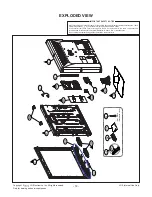
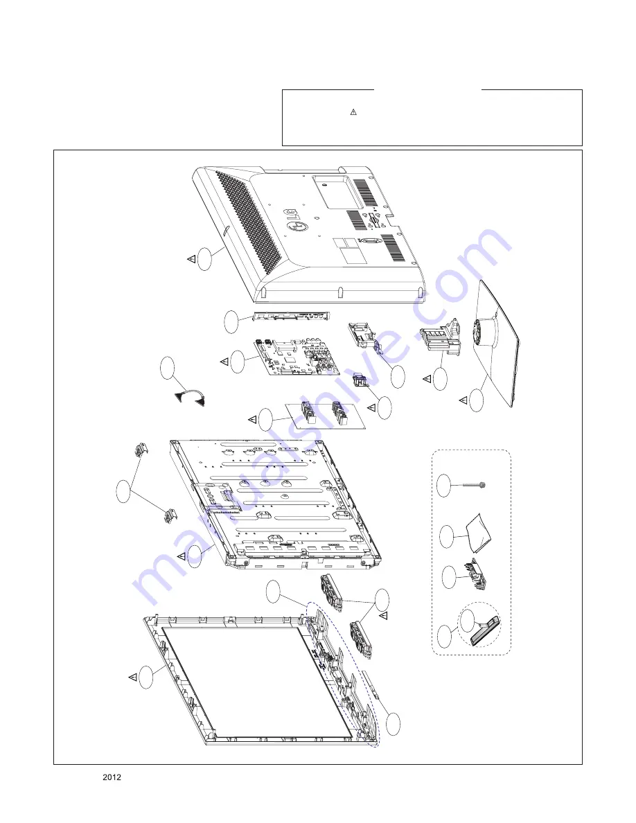
EXPLODED VIEW

Many electrical and mechanical parts in this chassis have special safety-related characteristics. These 

parts are identified by       in the Schematic Diagram and EXPLODED VIEW. 

It  is  essential  that  these  special  safety  parts  should  be  replaced  with  the  same  components  as 

recommended in this manual to prevent X-RADIATION, Shock, Fire, or other Hazards. 

Do not modify the original design without permission of manufacturer.

IMPORTANT SAFETY NOTICE

Summary of Contents for 22LS3500

Page 1: ...0T 463 465 MODEL 32CS460 460S 460T 463 465 ZA CAUTION BEFORE SERVICING THE CHASSIS READ THE SAFETY PRECAUTIONS IN THIS MANUAL LCD TV SERVICE MANUAL North Latin America http aic lgservice com Europe Africa http eic lgservice com Asia Oceania http biz lgservice com Internal Use Only ...

Page 2: ...lectronics Inc All rights reserved Only for training and service purposes CONTENTS CONTENTS 2 SAFETY PRECAUTIONS 3 SERVICING PRECAUTIONS 4 SPECIFICATION 6 ADJUSTMENT INSTRUCTION 10 BLOCK DIAGRAM 16 EXPLODED VIEW 19 SCHEMATIC CIRCUIT DIAGRAM ...

Page 3: ...inals etc to be sure the set is safe to operate without damage of electrical shock Leakage Current Cold Check Antenna Cold Check With the instrument AC plug removed from AC source connect an electrical jumper across the two AC plug prongs Place the AC switch in the on position connect one lead of ohm meter to the AC plug prongs tied together and touch other ohm meter lead in turn to each exposed m...

Page 4: ...lectrostatic charge on your body by touching a known earth ground Alter natively obtain and wear a commercially available discharging wrist strap device which should be removed to prevent poten tial shock reasons prior to applying power to the unit under test 2 After removing an electrical assembly equipped with ES devices place the assembly on a conductive surface such as aluminum foil to prevent...

Page 5: ...he solder joints of the two original leads If they are not shiny reheat them and if necessary apply additional solder Fuse and Conventional Resistor Removal Replacement 1 Clip each fuse or resistor lead at top of the circuit board hollow stake 2 Securely crimp the leads of replacement component around notch at stake top 3 Solder the connections CAUTION Maintain original spacing between the replace...

Page 6: ... Germany France Spain Sweden Finland Nether lands Belgium Luxemburg Greece Denmark Czech Austria Hungary Swiss Croatia Turkey Norway Slovenia Poland Ukraine Portugal Ireland Morocco Latvia Estonia Lithania Rumania Bulgaria Russia Slovakia Bosnia Serbia Albania Kazakhstan Belarus DTV MPEG2 4 DVB T2 8 countries UK Denmark Sweden Finland Norway Ireland Ukraine Kazakhstan DTV MPEG2 4 DVB C 37 countrie...

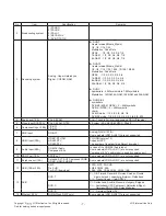
Page 7: ...rt RF OUT analog 5 Video Input RCA 1EA PAL SECAM NTSC 4 System PAL SECAM NTSC PAL60 6 Component Input 1EA Y Cb Cr Y Pb Pr 7 RGB Input RGB PC Analog D SUB 15PIN Some models LD21A LD21C are not supported 8 HDMI Input 3EA HDMI1 DTV DVI HDMI2 DTV HDMI3 DTV PC HDMI version 1 3 Support HDCP The number of Input ports is different by model 9 Audio Input 2EA RGB DVI Audio Component AV In case of the RGB DV...

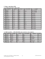
Page 8: ...96 59 94 74 176 HDTV 720P 10 1920 1080 28 125 50 00 74 25 HDTV 1080I 11 1920 1080 33 75 60 00 74 25 HDTV 1080I 12 1920 1080 33 72 59 94 74 176 HDTV 1080I 13 1920 1080 56 25 50 00 148 50 HDTV 1080P 14 1920 1080 67 50 60 00 148 50 HDTV 1080P 15 1920 1080 67 432 59 94 148 352 HDTV 1080P 16 1920 1080 27 00 24 00 74 25 HDTV 1080P 17 1920 1080 26 97 23 94 74 176 HDTV 1080P 18 1920 1080 33 75 30 00 74 25...

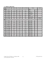
Page 9: ...0 020 108 0 VESA SXGA O FHD only 9 1920 1080 67 50 60 00 148 5 HDTV 1080P O FHD only DTV 1 720 480 31 47 59 94 27 00 SDTV 480P 2 720 480 31 50 60 00 27 027 SDTV 480P 3 720 576 31 250 50 00 27 00 SDTV 576P 4 1280 720 37 50 50 00 74 25 HDTV 720P 5 1280 720 45 00 60 00 74 25 HDTV 720P 6 1280 720 44 96 59 94 74 176 HDTV 720P 7 1920 1080 28 125 50 00 74 25 HDTV 1080I 8 1920 1080 33 75 60 00 74 25 HDTV ...

Page 10: ...fter downloading check OK message USB DOWNLOAD 1 Put the USB Stick to the USB socket 2 Automatically detecting update file in USB Stick If your downloaded program version in USB Stick is Low it didn t work But your downloaded version is High USB data is automatically detecting 3 Show the message Copying files from memory 4 Updating is starting 5 Updating Completed The TV will restart automatically...

Page 11: ...ustment The use of a internal pattern 0 1 2 3 4 5 6 7 8 9 A B C D E F 00 00 FF FF FF FF FF FF 00 1E 6D a b 10 c 01 03 68 A0 5A 78 0A EE 91 A3 54 4C 99 26 20 0F 50 54 A1 08 00 71 40 61 40 45 40 31 40 01 01 30 01 01 01 01 01 01 1B 21 50 A0 51 00 1E 30 48 88 40 35 00 40 84 00 00 00 1C 01 1D 00 72 51 D0 1E 20 50 6E 28 55 00 A0 5A 00 00 00 1E 00 00 00 FD 00 3A 60 3E 1F 46 10 00 0A 20 20 20 20 20 20 d 7...

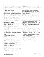
Page 12: ...b 00 00 White Balance Start Wb 00 ff White Balance End Caution Color Temperature COOL Medium Warm One of R Gain G Gain B Gain should be kept on 0xC0 and adjust other two lower than C0 When R G B Gain are all C0 it is the FULL Dynamic Range of Module Manual W B process using adjust Remote control After enter Service Mode by pushing ADJ key Enter White Balance by pushing key at 8 White Balance After...

Page 13: ...or 6 seconds 6 Confirm that ok pop up If change is not seen replace Eye Q II sensor 4 3 3D function test Pattern Generator MSHG 600 MSPG 6100 Support HDMI1 4 HDMI mode NO 872 pattern No 83 1 Please input 3D test pattern like below HDMI mode No 872 pattern No 83 2 When 3D OSD appear automatically then select OK key 3 Don t wear a 3D Glasses Check the picture like below 4 4 IR emitter inspection 1 S...

Page 14: ...b Address high 00 1F ADL EEPROM Sub Address low 00 FF Data Write data CS CMD LENGTH ADH ADL Data_1 Data_n Delay 20ms 6 2 Comand Set Description FOS Default write 7mode data write Vtotal V_Frequency Sync_Polarity Htotal Hstart Vstart 0 Phase Data write Model Name and Serial Number write in EEPROM 6 3 Method notice 1 Serial number D L is using of scan equipment 2 Setting of scan equipment operated b...

Page 15: ...click 1 Push the 2 MAC Address write At success Download check the OK 3 Start CI Key Download Push the 4 Check the OK or NG 7 2 LAN Inspection 7 2 1 Equipment Condition Each other connection to LAN Port of IP Hub and Jig 7 2 2 LAN inspection solution LAN Port connection with PCB Network setting at MENU Mode of TV Setting automatic IP Setting state confirmation If automatic setting is finished you ...

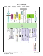
Page 16: ... V Rear TMDS DDR3 Add DDR3 Data SPI Side NAND FLASH IC102 2Gbit PCM_A 0 7 TMDS HDMI3 DDR3 1Gb IC1202 H5TQ1G63BFR DDR3 1Gb IC1201 H5TQ1G63BFR CONTROL IR LED SOFT TOUCH TACT SWITCH SENSOR _SCL SDA LED_R KEY1 KEY2 IR M24M01 HRMN6TP IC104 256Kbit I2C TMDS HDMI3 Except of LS3500 CS460 F SCART SC1_CVBS_IN SC1_R G B FE_ VOUT CI Slot 74LCX244 Buffer TS_DATA 0 7 PCM_DATA 0 7 FE_TS_DATA 0 7 PCM_A 8 14 Ether...

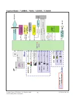
Page 17: ...b Pr L R RGB H V Rear TMDS DDR3 Add DDR3 Data SPI Side NAND FLASH IC102 2Gbit PCM_A 0 7 TMDS HDMI3 DDR3 1Gb IC1202 H5TQ1G63BFR DDR3 1Gb IC1201 H5TQ1G63BFR CONTROL IR LED SOFT TOUCH TACT SWITCH SENSOR _SCL SDA LED_R KEY1 KEY2 IR M24M01 HRMN6TP IC104 256Kbit I2C TMDS HDMI3 Except of LS350T CS460T F SCART SC1_CVBS_IN SC1_R G B FE_ VOUT CI Slot 74LCX244 Buffer TS_DATA 0 7 PCM_DATA 0 7 FE_TS_DATA 0 7 P...

Page 18: ...ear TMDS DDR3 Add DDR3 Data SPI Side NAND FLASH IC102 2Gbit PCM_A 0 7 TMDS HDMI3 DDR3 1Gb IC1202 H5TQ1G63BFR DDR3 1Gb IC1201 H5TQ1G63BFR CONTROL IR LED SOFT TOUCH TACT SWITCH SENSOR _SCL SDA LED_R KEY1 KEY2 IR M24M01 HRMN6TP IC104 256Kbit I2C TMDS HDMI3 Except of LS350S CS460S F SCART SC1_CVBS_IN SC1_R G B FE_ VOUT CI Slot 74LCX244 Buffer TS_DATA 0 7 PCM_DATA 0 7 FE_TS_DATA 0 7 PCM_A 8 14 Ethernet...

Page 19: ...any electrical and mechanical parts in this chassis have special safety related characteristics These parts are identified by in the Schematic Diagram and EXPLODED VIEW It is essential that these special safety parts should be replaced with the same components as recommended in this manual to prevent X RADIATION Shock Fire or other Hazards Do not modify the original design without permission of ma...

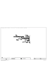
Page 20: ...D 3 VCC 2 RESET IC409 1 APX803D29 PD_ 24V_PWR_DET_DIODES 1 GND 3 VCC 2 RESET C436 0 01uF 50V 0 01uF C448 3300pF 50V C488 3300pF R403 1 5K 1 PD_ 24V R448 2 7K 1 PD_ 12V R450 0 5 PD_ 3 5V R473 1 R482 8 2K 1 PD_ 24V PWM1 R408 100 FOR 200HZ PWM_DIM2 R184 33 FOR LPB MODEL P407 12507WR 08L FOR LPB MODEL 1 2 3 4 5 6 7 8 9 R183 33 FOR LPB MODEL I2C_SDA I2C_SCL C409 0 015uF 50V 0 015uF Q400 MMBT3904 NXP E ...

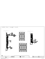
Page 21: ...al R704 10K OPT L702 70 ohm FHD L701 BLM18SG700TN1D 70 ohm HD AUO_GND LGD_NC LVDS_SEL 30Pin LVDS Connector For HD 60Hz_Normal LVDS for large inch 51Pin LVDS Connector For FHD 60Hz RXB3 RXA4 RXA0 RXB4 RXB1 RXB1 RXA4 RXB3 RXA4 RXA2 RXB3 RXB2 MIRROR FOR FHD REVERSE 8bit RXA0 RXA3 RXB0 RXA2 RXACK RXA1 RXA4 RXB1 RXB3 RXA2 RXB2 RXB4 RXB3 RXB0 MIRROR RXB3 RXB2 RXBCK RXACK RXB3 RXB1 RXA1 RXA0 RXB2 RXB4 RX...

Page 22: ...2 A4 P8 A5 P2 A6 R8 A7 R2 A8 T8 A9 R3 A10 AP L7 A11 R7 A12 BC N7 A13 T3 NC_5 M7 BA0 M2 BA1 N8 BA2 M3 CK J7 CK K7 CKE K9 CS L2 ODT K1 RAS J3 CAS K3 WE L3 RESET T2 DQSL F3 DQSL G3 DQSU C7 DQSU B7 DML E7 DMU D3 DQL0 E3 DQL1 F7 DQL2 F2 DQL3 F8 DQL4 H3 DQL5 H8 DQL6 G2 DQL7 H7 DQU0 D7 DQU1 C3 DQU2 C8 DQU3 C2 DQU4 A7 DQU5 A2 DQU6 B8 DQU7 A3 VREFCA M8 VREFDQ H1 ZQ L8 VDD_1 B2 VDD_2 D9 VDD_3 G7 VDD_4 K2 VD...

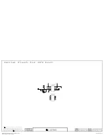
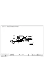
Page 23: ...4L_S7LR2 SPI_SCK 3 5V_ST 3 5V_ST C1401 0 1uF OS R1404 4 7K OPT SPI_CS SPI_SDO IC1401 MX25L8006EM2I 12G S_FLASH_MAIN_MACRONIX 3 WP 2 SO SIO1 4 GND 1 CS 5 SI SIO0 6 SCLK 7 HOLD 8 VCC R1405 33 OS R1403 10K OPT SPI_SDI FLASH_WP R1401 0 OPT IC1401 1 W25Q80BVSSIG S_FLASH_MAIN_WINBOND 3 WP IO2 2 DO IO1 4 GND 1 CS 5 DI IO0 6 CLK 7 HOLD IO3 8 VCC 3 5V_ST Q1401 MMBT3904 NXP OPT E B C Serial Flash for SPI bo...

Page 24: ...CM_A 1 CI_ADDR 2 CI_MDI 5 PCM_5V_CTL PCM_A 7 AR1908 33 CI_OE CI_ADDR 8 GND CI_OE CI_TS_CLK C1909 0 1uF CI_ADDR 7 CI_IORD CI_DATA 0 7 CI_ADDR 1 CI_MDI 3 PCM_A 11 CI_ADDR 6 P1902 10067972 050LF G1 G2 57 21 52 16 10 47 41 5 36 59 23 45 54 18 49 43 13 7 38 2 25 56 20 51 15 9 46 40 4 35 58 22 53 17 11 48 42 12 6 37 1 24 55 19 50 44 14 8 39 3 26 60 27 61 28 62 29 63 30 64 31 32 33 34 65 66 67 68 69 C190...

Page 25: ...21 GP4L_S7LR2 JK2100 XRJV 01V 0 D12 080 ETHERNET_XMULTIPLE 1 2 3 4 5 6 7 8 9 9 EPHY_RP JK2100 1 BS R430051 ETHERNET_UDE 1 1 2 2 3 3 4 4 5 5 6 6 7 7 8 8 9 9 EPHY_RN 2 5V_Normal EPHY_TN EPHY_TP L3707 BLM18PG121SN1D ETHERNET C2104 0 01uF 50V ETHERNET D2103 5 5V ADLC 5S 02 015 OPT D2104 5 5V ADLC 5S 02 015 OPT D2105 5 5V ADLC 5S 02 015 OPT D2101 5 5V ADLC 5S 02 015 OPT ETHERNET H W option ETHERNET Cop...

Page 26: ...2407 100pF 50V KEY2 C2410 0 1uF 16V OPT JP2409 3 5V_ST 3 5V_ST C2409 18pF 50V OPT LED_R BUZZ C2403 0 1uF 16V R2402 100 JP2408 R2412 100 C2401 0 1uF R2413 1 5K R2411 100 L2402 BLM18PG121SN1D JP2410 KEY1 C2404 1000pF 50V L2401 BLM18PG121SN1D IR P2400 12507WR 10L 1 2 3 4 5 6 7 8 9 10 11 R2404 10K 1 R2405 10K 1 3 5V_ST D2401 5 6V AMOTECH CO LTD OPT D2402 5 6V AMOTECH CO LTD OPT D2404 5 48VTO5 76V D240...

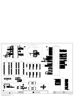
Page 27: ...9 0 1uF 16V DVB_S FE_TS_VAL 1 23V_TU C2615 10uF 10V DVB_S C2620 0 1uF 16V T2 C2632 10uF 10V DVB_S 3 3V_S2_DE TU2601 TDSQ G001D TU_T C S2 1 NC_1 2 RESET 3 SCL 4 SDA 5 B1 3 3V 6 SIF 7 B2 1 8V 8 CVBS 9 T C_IF_AGC 10 T C_DIF P 11 T C_DIF N 12 NC_2 13 NC_3 14 NC_4 15 GND_1 16 ERROR 17 SYNC 18 VALID 19 MCLK 20 D0 21 D1 22 D2 23 D3 24 D4 25 D5 26 D6 27 D7 28 GND_2 29 GND_3 30 B3 1 23V 31 S2_RESET 38 SHIE...

Page 28: ...IC2700 A8290SETTR T LNB 1 BOOST 3 TCAP 7 TDI 9 VREG 10 SDA 11 ADD 12 SCL 13 NC_2 14 IRQ 15 NC_3 16 NC_4 17 NC_5 18 NC_6 19 BFC 20 NC_7 21 NC_8 22 BFO 23 NC_9 24 BFI 25 VIN 26 LX 27 GNDLX 28 LNB 5 TDO 8 GND 6 EXTM 4 NC_1 2 VCP 29 EP C2708 0 22uF LNB C2701 0 01uF 50V LNB C2710 27pF OPT A_GND C2705 68uF 35V LNB A_GND R2706 0 R2705 0 D2700 40V SX34 LNB D2702 40V SX34 LNB C2712 0 1uF 50V LNB A_GND ZD1 ...

Page 29: ... AUD_LRCK SPK_L C3403 0 1uF 16V C3407 0 1uF 16V AUD_SCK C3417 10uF 35V C3400 0 1uF 50V C3411 0 1uF 50V R3410 43 C3422 0 22uF 50V 24V C3416 0 1uF 50V 3 3V_AMP C3419 0 22uF 50V L3404 10 0uH 3 5V_ST Q3400 MMBT3904 NXP NON_LIPS E B C R3409 43 AMP_MUTE 24V_AMP C3413 330pF 50V C3414 330pF 50V C3426 1000pF 50V C3427 1000pF 50V C3425 1000pF 50V C3424 1000pF 50V C3415 1uF 50V C3412 1uF 50V L3400 CIS21J121 ...

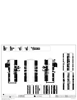
Page 30: ...RXB4 3 3V_Normal PCM_OE RL_ON 3 3V_Normal PF_CE0 RXA3 USB1_CTL 3 3V_Normal R146 33 PF_OE R118 1K AUD_MASTER_CLK_0 PWM2 C103 0 1uF OS MODEL_OPT_7 C109 0 1uF RXA0 PM_MODEL_OPT_0 R147 33 3 3V_Normal R164 22 EU_OPT FE_TS_VAL_ERR 5V_DET_HDMI_1 IC102 1 H27U1G8F2BTR BC NAND_FLASH_1G_HYNIX EAN35669102 26 NC_17 27 NC_18 28 NC_19 29 I O0 30 I O1 31 I O2 32 I O3 33 NC_20 34 NC_21 35 NC_22 36 VSS_2 37 VCC_2 3...

Page 31: ... AVDD_MOD_1 V18 AVDD_MOD_2 U19 AVDD25_PGA W14 AVSS_PGA W15 AVDD_NODIE U7 AVDD_DVI_USB_1 L7 AVDD_DVI_USB_2 M7 AVDD3P3_MPLL P7 AVDD_DMPLL R7 DVDD_NODIE M19 AVDD_AU33 V7 AVDD_EAR33 W7 VDDP_1 R19 VDDP_2 T19 AVDD_LPLL_1 W18 AVDD_LPLL_2 W19 VDDP_NAND V19 AVDD_DDR0_D_1 J17 AVDD_DDR0_D_2 K15 AVDD_DDR0_D_3 K16 AVDD_DDR0_C L15 AVDD_DDR1_D_1 K17 AVDD_DDR1_D_2 L17 AVDD_DDR1_D_3 M17 AVDD_DDR1_C L16 GND_EFUSE E...

Page 32: ... AP2191DSG EAN61849601 3 IN_2 2 IN_1 4 EN 1 GND 5 FLG 6 OUT_1 7 OUT_2 8 NC SIDE_USB1_DM C1453 0 1uF C1452 10uF 10V USB1_CTL R1455 4 7K OPT R1454 10K L1451 CIS21J121 3 3V_Normal SIDE_USB1_DP 5V_USB C1451 22uF 16V R1451 47 JK1450 3AU04S 305 ZC LG USB_1_NORMAL 1 2 3 4 5 L1451 1 MLB 201209 0120P N2 120 ohm USB1_OCD D1451 RCLAMP0502BA OPT R1458 2K 1 8W 5 OPT R1459 2K 1 8W 5 OPT JK1450 1 3AU04S 345 ZC H...

Page 33: ...HDMI_CEC D0 _HDMI2 HDMI_CEC D1 _HDMI1 5V_HDMI_1 R885 2 7K HDMI_2 5V_HDMI_2 DDC_SDA_2 R802 3 3K R828 10K HDMI_2 D1 _HDMI1 R803 1 8K HDMI_2 DDC_SDA_1 D0 _HDMI1 D0 _HDMI2 D0 _HDMI1 D1 _HDMI2 DDC_SCL_2 5V_DET_HDMI_2 5V_Normal 5V_DET_HDMI_1 R896 1K 5V_Normal D2 _HDMI1 D2 _HDMI1 DDC_SDA_2 CK _HDMI1 C802 0 1uF 16V NON_CI_CAP D2 _HDMI2 CK _HDMI1 HPD2 R805 0 HDMI_ARC CK _HDMI2 R889 2 7K HDMI_2 R806 10K DDC...

Page 34: ...NV_IN3 11 GND 12 NON_INV_IN4 13 INV_IN4 14 OUT4 DTV MNT_L_OUT R2832 10K R2831 10K C2816 0 1uF EU_OPT SC1 COMP1_L_IN L2802 120 ohm EU_OPT COMP2_Pb SC1_G COMP1_Y R2842 1K R2869 10K EU_OPT C2824 33pF EU_OPT COMP2_DET SC1 COMP1_R_IN SC1_CVBS_IN R2812 10K EU_OPT L2804 EU_OPT C2814 0 1uF 50V EU_OPT R2818 12K EU_OPT R2826 470K JK2801 PSC008 01 EU_OPT 1 AUDIO_R_OUT 2 AUDIO_R_IN 3 AUDIO_L_OUT 4 AUDIO_GND 5...

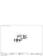
Page 35: ...IF IS ESSENTIAL THAT ONLY MANUFATURES SPECFIED PARTS BE USED FOR THE CRITICAL COMPONENTS IN THE SYMBOL MARK OF THE SCHEMETIC 2011 09 26 RS232C_4PIN 57 GP4L_S7LR2 PM_TXD PM_RXD 3 5V_ST P1000 12507WS 04L 1 VCC 2 PM_RXD 3 GND 4 PM_TXD 5 GND RS 232C 4PIN Copyright 2012 LG Electronics Inc All rights reserved Only for training and service purposes LGE Internal Use Only ...

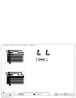
Page 36: ...IF IS ESSENTIAL THAT ONLY MANUFATURES SPECFIED PARTS BE USED FOR THE CRITICAL COMPONENTS IN THE SYMBOL MARK OF THE SCHEMETIC 2011 09 05 MSTAR DEBUG_4PIN 58 GP4L_S7LR2 RGB_DDC_SCL RGB_DDC_SDA P1 12505WS 04A00 MSTAR_DEBUG_4P 1 2 3 4 5 MSTART DEBUG_4PIN Copyright 2012 LG Electronics Inc All rights reserved Only for training and service purposes LGE Internal Use Only ...

Page 37: ......
Page 38: ...error No power 7 7 Off when on off while viewing power auto on off 8 8 C Audio error No audio Normal video 9 9 Wrecked audio discontinuation noise 10 10 D Function error Remote control Local switch checking 11 11 External device recognition error 12 12 E Noise Circuit noise mechanical noise 13 13 F Exterior error Exterior defect 14 First of all Check whether there is SVC Bulletin in GCSC System fo...

Page 39: ...7 10 Check Link Cable LVDS reconnection condition A8 A9 11 Adjustment Test pattern ADJ Key A10 12 A Video error_Vertical Horizontal bar residual image light spot LCD TV connection diagram A8 13 Check Link Cable LVDS reconnection condition A8 A9 14 Adjustment Test pattern ADJ Key A10 15 Appendix Defected Type caused by T Con Inverter Module Exchange T Con Board 1 A 1 5 16 Exchange T Con Board 2 A 2...

Page 40: ...ck record S W Version and White Balance value before replacing the Main Board Replace Main Board Re enter White Balance value Precaution Established date Standard Repair Process Revised date 1 14 LCD TV Error symptom A Video error No video Normal audio A4 A1 A2 A6 A3 First of all Check whether all of cables between board is inserted properly or not Main B D Power B D LVDS Cable Speaker Cable IR B ...

Page 41: ...replace MAIN B D Y Replace Power Board and repair parts N End Standard Repair Process A Video error No video No audio A4 Established date Revised date 2 14 LCD TV Error symptom 2012 01 14 Copyright 2012 LG Electronics Inc All rights reserved Only for training and service purposes LGE Internal Use Only ...

Page 42: ...ck Tuner soldering Normal Picture Y N Y Close Normal Picture Y Close By using Digital signal level meter By using Diagnostics menu on OSD Menu Set up Support Signal Test Signal strength Normal over 50 Signal Quality Normal over 50 Normal Picture Y Contact with signal distributor or broadcaster Cable or Air N N Normal Picture Y Close N A6 Standard Repair Process Established date Revised date 3 14 L...

Page 43: ...t maker TV etc Y Change satellite setting match with installed ANT N Normal Picture Y Close N A6 Standard Repair Process Established date Revised date 4 14 LCD TV Error symptom 2012 01 14 Check satellite setting Check LNB frequency Check satellite Check Satellite connection DiSEqC motor etc Normal setting Contact with signal distributor or broadcaster Cable or Air Close N Check Tuner soldering Rep...

Page 44: ...vice and cable Y External device Cable normal RGB HDMI DVI error Check external device and cable Replace Main B D Replace Main B D N N A Video error Color error A7 N Y End Replace module Request repair for external device cable Color error Check Test pattern A10 A8 A9 Standard Repair Process Established date Revised date 5 14 LCD TV Error symptom 2012 01 14 Copyright 2012 LG Electronics Inc All ri...

Page 45: ...g Jig pattern Generator Set top Box etc N Y Replace Main B D Screen normal Check screen condition by input External Input Component RGB HDMI DVI Request repair for external device Component error RGB error HDMI DVI Connect other external device and cable Check normal operation of External Input Component RGB and HDMI DVI by connecting Jig pattern Generator Set top Box etc Replace Main B D Screen n...

Page 46: ...ltage of each output of Power B D N Y Normal voltage Replace Main B D N Y OK Replace Main B D N Y Normal Check ST BY 3 5V Replace Power B D N Y Normal voltage Replace Power B D Y A11 A12 A13 A4 Standard Repair Process Established date Revised date 7 14 LCD TV Error symptom Stand By Red Close 2012 01 14 Copyright 2012 LG Electronics Inc All rights reserved Only for training and service purposes LGE...

Page 47: ...by REMOTE CONTROL POWEROFF_OFFTIMER Power off by OFF TIMER POWEROFF_SLEEPTIMER Power off by SLEEP TIMER POWEROFF_INSTOP Power off by INSTOP KEY POWEROFF_AUTOOFF Power off by AUTO OFF POWEROFF_ONTIMER Power off by ON TIMER POWEROFF_RS232C Power off by RS232C POWEROFF_RESREC Power off by Reserved Record POWEROFF_RECEND Power off by End of Recording POWEROFF_SWDOWN Power off by S W Download POWEROFF_...

Page 48: ...repair parts Check Speaker disconnection N Y Replace Speaker Replace MAIN Board End C Audio error No audio Normal video A15 A16 Disconnection Established date Revised date 9 14 LCD TV Error symptom Standard Repair Process 2012 01 14 Copyright 2012 LG Electronics Inc All rights reserved Only for training and service purposes LGE Internal Use Only ...

Page 49: ...ct and check other external device N Y Normal audio Check and fix external device Replace Power B D N Y Normal voltage Check input signal RF External Input signal Signal normal When RF signal is not received Request repair to external cable ANT provider Y Check audio B Voltage 24V Replace Main B D In case of External Input signal error Check and fix external device Replace Main B D N End Establish...

Page 50: ...rry of R C Check Repair Cable connection Connector solder Normal operating Check B 3 5V On Main B D A17 Normal Voltage Close N N Check 3 5v on Power B D Replace Power B D or Replace Main B D Power B D don t have problem A4 Check IR Output signal Normal Signal N Y Repair Replace IR B D N A17 Replace Main B D Y A17 Standard Repair Process Established date Revised date 11 14 LCD TV Error symptom 2012...

Page 51: ... device cable RGB HDMI DVI Optical Recognition error Replace Main B D Replace Main B D Fix in accordance with technical information D Function error External device recognition error Established date Revised date 12 14 LCD TV Error symptom Standard Repair Process 2012 01 14 Copyright 2012 LG Electronics Inc All rights reserved Only for training and service purposes LGE Internal Use Only ...

Page 52: ...s shown in the solution manual For models without any fix information provide the description OR Mechanical noise is a natural phenomenon and apply the 1st level description When the customer does not agree apply the process by stage Describe the basis of the description in Part related to nose in the Owner s Manual E Noise Circuit noise mechanical noise Established date Revised date 13 14 LCD TV ...

Page 53: ...te controller Remote controller damage Stand dent Replace stand F Exterior defect Exterior defect Established date Revised date 14 14 LCD TV Error symptom Standard Repair Process 2012 01 14 Copyright 2012 LG Electronics Inc All rights reserved Only for training and service purposes LGE Internal Use Only ...

Reviews: