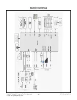
THERMAL
THERMAL
THE SYMBOL MARK OF THIS SCHEMETIC DIAGRAM INCORPORATES
SPECIAL FEATURES IMPORTANT FOR PROTECTION FROM X-RADIATION.
FILRE AND ELECTRICAL SHOCK HAZARDS, WHEN SERVICING IF IS
ESSENTIAL THAT ONLY MANUFATURES SPECFIED PARTS BE USED FOR
THE CRITICAL COMPONENTS IN THE SYMBOL MARK OF THE SCHEMETIC.
SIGN1100165
HP_LOUT_MAIN
HP_ROUT_AMP
+3.3V_NORMAL
HP_LOUT_AMP
HP_ROUT_MAIN
SIDE_HP_MUTE
+3.3V_NORMAL
AUD_LRCK
SPK_R+
SPK_R+
+19V_AMP
AUD_LRCH
I2C_SDA1
SPK_L-
+3.3V_NORMAL
AUD_MASTER_CLK
AUD_SCK
SPK_R-
+19V_AMP
+3.3V_NORMAL
SPK_L-
AMP_RESET_N
+19V_AMP
SPK_L+
AMP_MUTE
SPK_L+
+19V
SPK_R-
I2C_SCL1
D6903-*1
40V
LNB_SX34
D6904-*1
40V
LNB_SX34
I2C_SDA4
LNB_OUT
A_GND
A_GND
I2C_SCL4
A_GND
A_GND
LNB_TX
A_GND
+12V
A_GND
L5405-*1
NRS6045T100MMGK
Audio_Coil_TAIYO
10.0uH
L5403-*1
NRS6045T100MMGK
Audio_Coil_TAIYO
10.0uH
L5402-*1
NRS6045T100MMGK
Audio_Coil_TAIYO
10.0uH
L5404-*1
NRS6045T100MMGK
Audio_Coil_TAIYO
10.0uH
+3.3V_NORMAL
+3.3V_NORMAL
SMARTCARD_CLK/SD_EMMC_DATA[0]
+5V_NORMAL
+3.3V_NORMAL
SMARTCARD_RST/SD_EMMC_DATA[2]
SMARTCARD_DET/SD_EMMC_DATA[3]
SMARTCARD_DATA/SD_EMMC_CLK
+3.3V_NORMAL
SMARTCARD_PWR_SEL/SD_EMMC_DATA[1]
SMARTCARD_VCC/SD_EMMC_CMD
L6100
120-ohm
BLM18PG121SN1D
C6104
180pF
C6109
180pF
C6101
1uF
10V
C6100
1uF
10V
R6105
4.7K
R6104
43K
1%
C6103
1uF
10V
C6105
1uF
10V
C6102
1uF
10V
C6107
0.1uF
16V
R6106
43K
1%
0.1uF
C5400
50V
R5403
100
0.1uF
C5437
50V
R5408
12
R5416
5.1K
R5411
12
C5414
10uF
10V
C5424
0.01uF
50V
OPT
R5400
10K
R5402
100
R5415
5.1K
C5440
0.1uF
16V
OPT
T
P
5
4
0
2
C5417
22000pF
50V
0.1uF
C5439
50V
C5430
390pF
50V
R5409
12
R5401
10K
0.1uF
C5436
50V
C5429
390pF
50V
R5414
12
C5411
0.1uF
16V
0.1uF
C5401
50V
C5427
1uF
10V
0.1uF
C5419
50V
C5425
22000pF
50V
C5416
22000pF
50V
C5406
33pF
50V
R5406
3.3
OPT
R5405
100
0.1uF
C5438
50V
Q5400
MMBT3904(NXP)
E
B
C
R5412
12
P5400
WAFER-ANGLE
1
2
3
4
0.1uF
C5421
50V
C5408
33pF
50V
T
P
5
4
0
1
C5435
0.47uF
50V
C5433
1uF
10V
C5431
390pF
50V
C5428
1uF
10V
R5417
5.1K
R5410
12
0.1uF
C5413
16V
C5426
22000pF
50V
T
P
5
4
0
0
0.1uF
C5420
50V
R5413
12
R5418
5.1K
C5434
0.47uF
50V
C5404
1000pF
50V
C5432
390pF
50V
L5401
BLM18PG121SN1D
0.1uF
C5418
50V
R5407
12
C5415
1000pF
50V
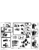
C6904
0.1uF
50V
LNB
C6903
0.01uF
50V
LNB
D6903
40V
LNB_SMAB34
SMAB34
C6905
10uF
25V
LNB
L6900
15uH
SP-7850_15
LNB
D6901
30V
MBR230LSFT1G
LNB
R6900
2.2K
1W
LNB
C6908
0.1uF
LNB
C6909
10uF
25V
LNB
C6906
10uF
25V
LNB
R6903
39K
1/16W
1%
LNB
C6910
0.1uF
50V
LNB
C6907
10uF
25V
LNB
C6900
18pF
LNB
C6901
33pF
LNB
C6902
0.22uF
25V
LNB
R6901
33
LNB
R6902
33
LNB
C6911
0.22uF
LNB
D6902
30V
LNB
D6904
40V
LNB_SMAB34
R6904
0
C6912
0.1uF
LNB
D6900
LNB
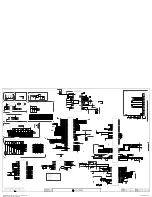
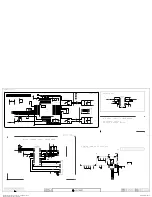
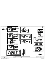
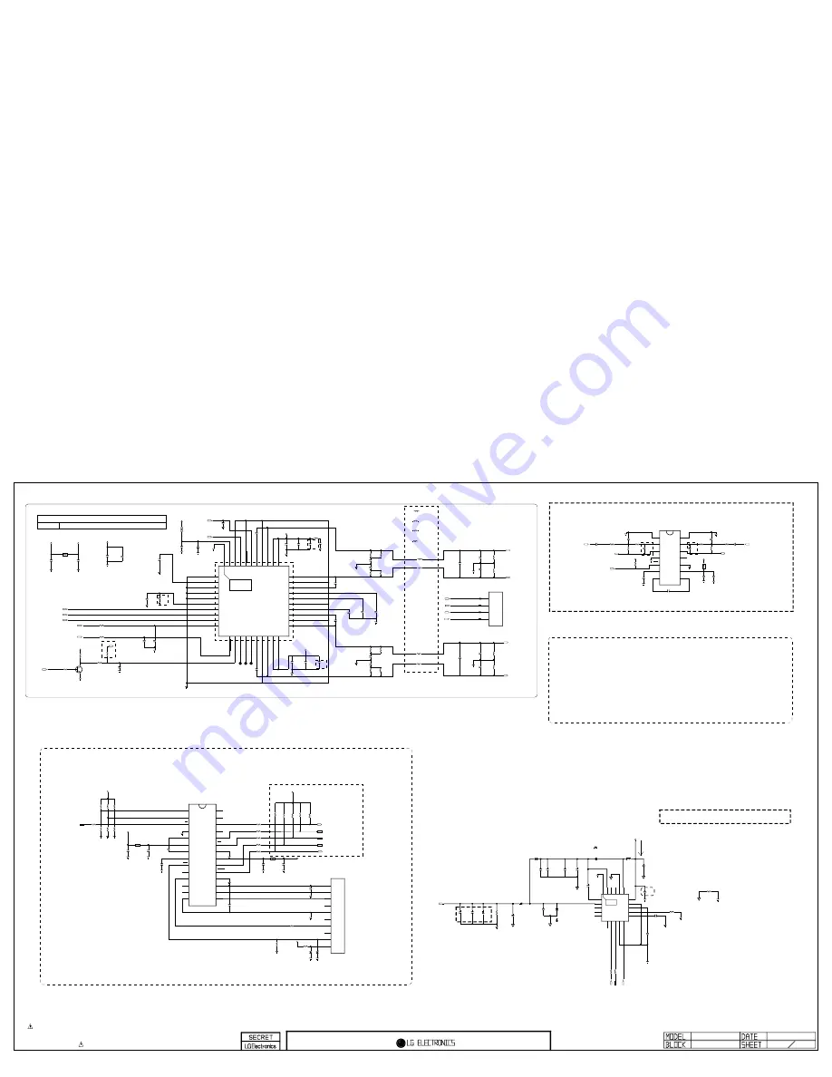
IC8101
NTP7513
3
DGND_PLL
2
VDD_PLL
4
GND
1
AGND_PLL
6
DVDD
5
DGND
7
SDATA
8
WCK
9
BCK
10
SDA
11
SCL
12
FAULT
13
MONITOR_0
14
MONITOR_1
15
MONITOR_2
16
BST2B
17
PGND2B
18
OUT2B
19
PVDD2B
20
PVDD2A
21
OUT2A
22
PGND2A
23
BST2A
24
VDR2
25
AGND
26
VCC5
27
VDR1
28
BST1B
29
PGND1B
30
OUT1B
31
PVDD1B
32
PVDD1A
33
OUT1A
34
PGND1A
35
BST1A
36
RESET
37
AD
38
CLK_I
39
GND_IO
40
VDD_IO
41
[EP]GND
L5404
LPH6045T-100M
Audio_Coil_ABCO
10uH
L5405
LPH6045T-100M
Audio_Coil_ABCO
10uH
L5402
LPH6045T-100M
Audio_Coil_ABCO
10uH
L5403
LPH6045T-100M
Audio_Coil_ABCO
10uH
1uF
C5412
10V
IC6100
TPA6138A2
3
OUTR
2
-INR
4
GND_1
1
+INR
6
VSS
5
MUTE
7
CN
8
CP
9
VDD
10
GND_2
11
UVP
12
OUTL
13
-INL
14
+INL
C6303
0.1uF
16V
JAPAN
C6302
0.1uF
16V
JAPAN
P6300
10057542-1311FLF(B CAS Slot)
JAPAN
C1
VCC
C2
RST
C3
CLK
C4
RESERVED_1
C5
GND
C6
VPP
C7
I/O
C8
RESERVED
S1
SW1
S2
SW2
R6316
1.2K
JAPAN
R6315
1.2K
JAPAN
R6311
22
JAPAN
L6301
BLM18PG121SN1D
JAPAN
ZD6301
5V
JAPAN
R6305
2.7K
JAPAN
R6313
75
JAPAN
R6307
22
JAPAN
R6317
1.2K
OPT
R6309
22
JAPAN
R6306
OPT
C6304
0.1uF
16V
JAPAN
C6306
0.1uF
16V
JAPAN
IC6300
TDA8024TT
JAPAN
3
5V/3V
2
CLKDIV2
4
PGND
1
CLKDIV1
6
VDDP
5
S2
7
S1
8
VUP
9
PRES
10
PRES
11
I/O
12
AUX2
13
AUX1
14
CGND
15
CLK
16
RST
17
VCC
18
PORADJ
19
CMDVCC
20
RSTIN
21
VDD
22
GND
23
OFF
24
XTAL1
25
XTAL2
26
I/OUC
27
AUX1UC
28
AUX2UC
C6305
0.1uF
16V
JAPAN
R6302
OPT
ZD6300
5V
JAPAN
R6303
2.7K
OPT
R6312
10K
JAPAN
R6304
2.7K
JAPAN
R6314
1K
JAPAN
R6301
2.7K
JAPAN
C6307
0.33uF
16V
JAPAN
R6308
22
JAPAN
R6310
22
JAPAN
C6301
10uF
10V
JAPAN
R6300 22
JAPAN
C6300
0.1uF
16V
JAPAN
L6300
BLM18PG121SN1D
JAPAN
C5422
10uF
25V
C5423
10uF
25V
IC6900
A8303SESTR-T
LNB
1
VCP
3
NC_1
7
SCL
9
ADD
10
TONECTRL
11
TCAP
12
ISET
13
VREG
14
GND
15
VIN
16
LX
17
GNDLX
18
NC_2
19
NC_3
20
BOOST
5
TDO
8
SDA
6
IRQ
4
TDI
2
LNB
21
[EP]GND
C6106
10pF
50V
C6108
10pF
50V
R6319
1.2K
OPT
R6318
1.2K
JAPAN
R5419
100
OPT
POWER_DET
C5402
10uF
35V
OPT
+19V_AMP
C5403
10uF
35V
OPT
L5400
UBW2012-121F
R6103
12K
R6102
12K
R6100
10K
R6101
10K
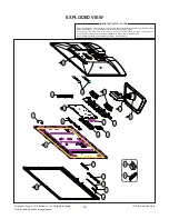
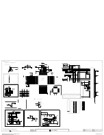
EARPHONE AMP
1ST : 0TRIY80001A 2ND : 0TR387500AA
AUDIO AMP
SPEAKER_L
Q1801
DUAL COMPONENT
SPEAKER_R
0x54
RS-232C Control INTERFACE
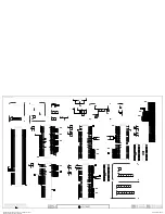
Surge protectioin
3.5A
Caution!! need isolated GND
Ouput trace widths should be sized to conduct at least 2A
Close to Tuner
3A
close to VIN pin(#15)
(Option:LNB)
close to Boost pin(#1)
Max 1.3A
Input trace widths should be sized to conduct at least 3A
2A
DVB-S2 LNB Part Allegro
20120813 CJ.LIM
T-NTP7513->EAN62653101
20120813 LCD-TV
Delete diodes
20120813 LCD-TV
20120813 LCD-TV
Delete RS232C block
LN4600
2013.01.02
5 8
AUDIO/HP/LNB/B-CAS
20120816 CJ.LIM
LCD-TV
B-CAS (SMART CARD) INTERFACE
B-CAS SLOT
Place CLK C3 far from C2,C7,C4 and C8
CLKDIV1 CLKDIV2 : F_CRD_CLK
-----------------------------
1 0 CLKIN
75 ohm in I/O is for short circuit Protection
INT CMDVCC : STATUS
---------------------------------
HIGH HIGH CARD PRESENT
LOW HIGH CARD not PRESENT
20120913 CJLIM
ADD B-CAS CARD SLOT
EAX65085301
20121010 CJLIM
3225 -> 3216
20121010 CJLIM
3225 -> 3216
2012.10.16 LCD-TV
2012.10.16 LCD-TV
2012.10.17 LCD-TV
[DV2]
Copyright © 2013 LG Electronics. Inc. All rights reserved.
Only for training and service purposes
LGE Internal Use Only
Summary of Contents for 26LN46 -Z Series
Page 28: ......