background image

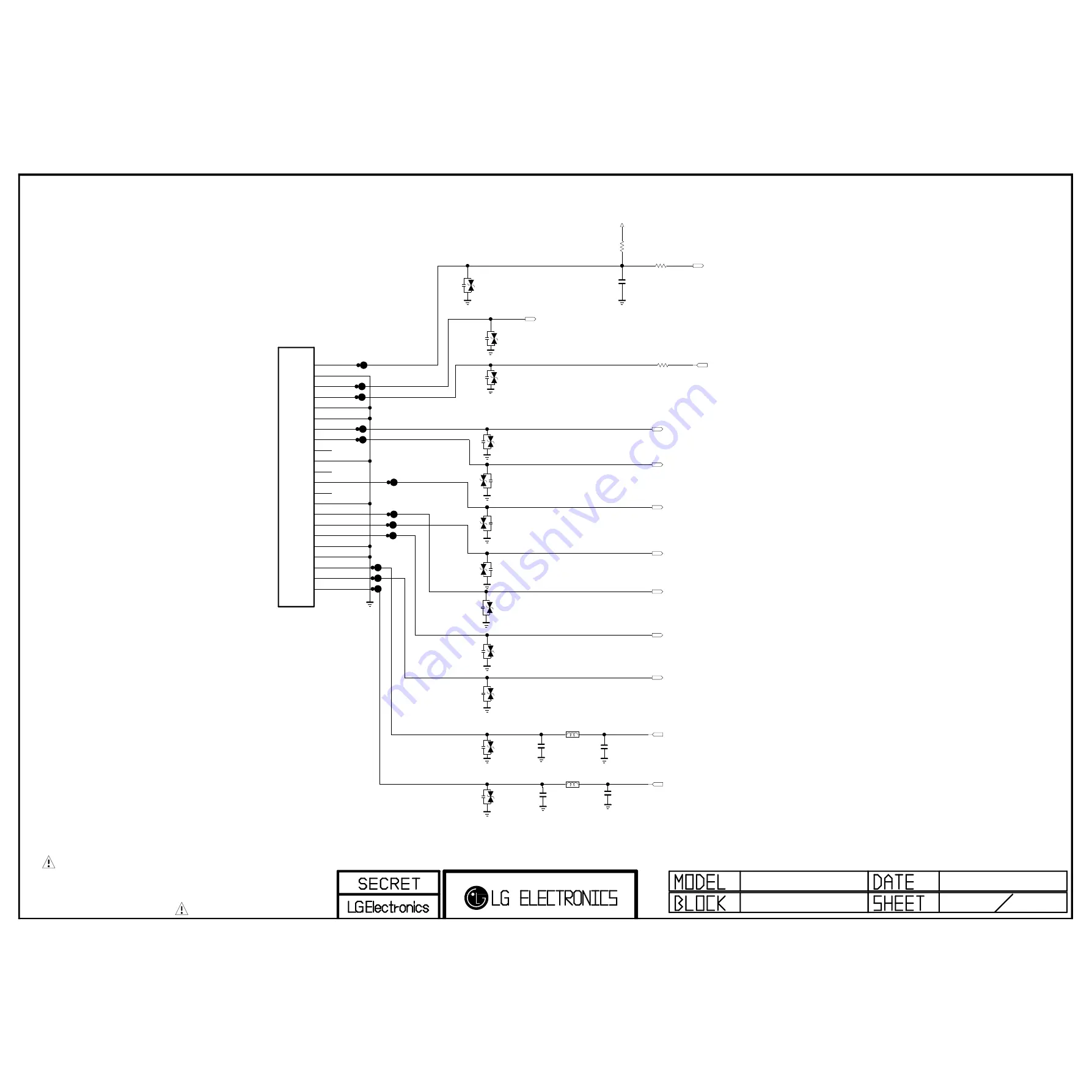
THE    SYMBOL MARK OF THIS SCHEMETIC DIAGRAM INCORPORATES
SPECIAL FEATURES IMPORTANT FOR PROTECTION FROM X-RADIATION.
FIRE AND ELECTRICAL SHOCK HAZARDS, WHEN SERVICING IF IS 
ESSENTIAL THAT ONLY MANUFACTURES SPECIFIED PARTS BE USED FOR
THE CRITICAL COMPONENTS IN THE    SYMBOL MARK OF THE SCHEMETIC.

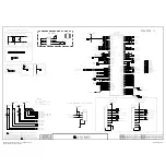
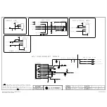
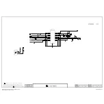
SC_FB

SC_R_IN

SC_G

VA4602
5.6V

EU

SC_B

DTV/MNT_L_OUT

SC_R

C4601

1000pF

50V

EU

VA4601

5.6V

EU

L4601

BLM18PG121SN1D

EU

VA4609

5.5V

EU

VA4610

5.5V

EU

VA4607

5.6V

EU

L4600

BLM18PG121SN1D

EU

SC_L_IN

VA4603
5.5V

EU

C4603
4700pF

EU

VA4608

5.6V

EU

JK4600

PSC008-01

EU

1

AUDIO_R_OUT

2

AUDIO_R_IN

3

AUDIO_L_OUT

4

AUDIO_GND

5

B_GND

6

AUDIO_L_IN

7

B_OUT

8

ID

9

G_GND

10

D2B_IN

11

G_OUT

12

D2B_OUT

13

R_GND

14

RGB_GND

15

R_OUT

16

RGB_IO

17

SYNC_GND1

18

SYNC_GND2

19

SYNC_OUT

20

SYNC_IN

21

COM_GND

22

AV_DET

C4604
0.1uF

EU

VA4600

20V

EU

+3.3V_NORMAL

VA4605

5.5V

EU

R8904

75

1/16W

EU

C4602
4700pF

EU

R4601

10K

EU

VA4611
5.6V

EU

VA4606

5.6V

EU

DTV/MNT_R_OUT

VA4604

5.5V

EU

SC_ID

R4602
100

EU

SC_CVBS_IN

C4600

1000pF
50V

EU

SC_DET

DTV/MNT_V_OUT

CLOSE TO JUNCTION

PAGE 15

Full Scart

Copyright © 2014 LG Electronics. Inc. All rights reserved. 

Only for training and service purposes

LGE Internal Use Only

Summary of Contents for 32LB65 Series

Page 1: ...B MODEL 32LB65 32LB65 Z CAUTION BEFORE SERVICING THE CHASSIS READ THE SAFETY PRECAUTIONS IN THIS MANUAL LED TV SERVICE MANUAL North Latin America http aic lgservice com Europe Africa http eic lgservice com Asia Oceania http biz lgservice com Internal Use Only ...

Page 2: ...lectronics Inc All rights reserved Only for training and service purposes CONTENTS CONTENTS 2 SAFETY PRECAUTIONS 3 SERVICING PRECAUTIONS 4 SPECIFICATION 6 ADJUSTMENT INSTRUCTION 13 BLOCK DIAGRAM 21 EXPLODED VIEW 22 SCHEMATIC CIRCUIT DIAGRAM ...

Page 3: ...inals etc to be sure the set is safe to operate without damage of electrical shock Leakage Current Cold Check Antenna Cold Check With the instrument AC plug removed from AC source connect an electrical jumper across the two AC plug prongs Place the AC switch in the on position connect one lead of ohm meter to the AC plug prongs tied together and touch other ohm meter lead in turn to each exposed m...

Page 4: ...ctrostatic charge on your body by touching a known earth ground Alter natively obtain and wear a commercially available discharg ing wrist strap device which should be removed to prevent potential shock reasons prior to applying power to the unit under test 2 After removing an electrical assembly equipped with ES devices place the assembly on a conductive surface such as aluminum foil to prevent e...

Page 5: ...he solder joints of the two original leads If they are not shiny reheat them and if necessary apply additional solder Fuse and Conventional Resistor Removal Replacement 1 Clip each fuse or resistor lead at top of the circuit board hollow stake 2 Securely crimp the leads of replacement component around notch at stake top 3 Solder the connections CAUTION Maintain original spacing between the replace...

Page 6: ...tries Germany Netherland Switzerland Hungary Austria Slov enia Bulgaria France Spain Italy Belgium Luxemburg Greece Czech Croatia Turkey Moroco Ireland Latvia Estonia Lithuania Poland Portugal Romania Albania Bosnia Serbia Slovakia Beralus DTV MPEG2 4 DVB T2 8 countries UK Ireland Sweden Denmark Finland Norway Ukraine Kazakhstan Russia DTV MPEG2 4 DVB C 37 countries Germany Netherland Switzerland ...

Page 7: ...2 2 5 2 3 3 4 5 6 64 QAM 1 2 2 5 2 3 3 4 5 6 256 QAM 1 2 2 5 2 3 3 4 5 6 DVB C Symbolrate 4 0Msymbols s to 7 2Msymbols s Modulation 16QAM 64 QAM 128 QAM and 256 QAM DVB S S2 symbolrate DVB S2 8PSK QPSK 2 45Msymbol s DVB S QPSK 2 45Msymbol s viterbi DVB S mode 1 2 2 3 3 4 5 6 7 8 DVB S2 mode 1 2 2 3 3 4 3 5 4 5 5 6 8 9 9 10 5 Scart 1EA PAL SECAM Scart 1 Jack is Full scart and support ATV DTV OUT no...

Page 8: ...80i 2 720 480 15 63 59 94 SDTV DVD 480i 3 720 480 31 47 59 94 480p 4 720 480 31 50 60 00 480p 5 720 576 15 625 50 00 SDTV DVD 625 Line 6 720 576 31 25 50 00 HDTV 576p 7 1280 720 45 00 50 00 HDTV 720p 8 1280 720 44 96 59 94 HDTV 720p 9 1280 720 45 00 60 00 HDTV 720p 10 1920 1080 31 25 50 00 HDTV 1080i 11 1920 1080 33 75 60 00 HDTV 1080i 12 1920 1080 33 72 59 94 HDTV 1080i 13 1920 1080 56 250 50 HDT...

Page 9: ...68 60Hz 47 712 60 015 VESA WXGA 9 1920 x 1080 60Hz 67 5 60 00 WUXGA Reduced Blanking 6 HDMI Input 6 1 DTV mode No Resolution H freq kHz V freq Hz Pixel clock MHz 1 640 480 31 469 31 5 59 94 60 SDTV 480P 2 720 480 31 469 31 5 59 94 60 SDTV 480P 3 720 576 31 25 50 SDTV 576P 4 720 576 15 625 50 SDTV 576I 5 1280 720 37 500 50 HDTV 720P 6 1280 720 44 96 45 59 94 60 HDTV 720P 7 1920 1080 33 72 33 75 59 ...

Page 10: ... 35 148 5 4 Side by side Full HDTV 720P 16 1920 1080 33 72 33 75 59 94 60 74 18 74 25 5 Top and Bottom Side by side half Secondary HDTV 1080I Primary HDTV 1080I 17 67 432 67 50 59 94 60 148 35 148 5 5 Frame packing Field alternative Primary HDTV 1080I HDTV 1080I 18 33 72 33 75 59 94 60 148 35 148 5 5 Side by side Full HDTV 1080I 19 28 125 50 00 74 25 20 Top and Bottom Side by side half Secondary H...

Page 11: ...0I 7 1920 1080 27 00 24 00 74 25 HDTV 1080P 2D to 3D Side by Side Half Top Bot tom Checker Board Row Interleaving Column Interleaving 8 1920 1080 28 12 25 74 25 HDTV 1080P 9 1920 1080 33 75 30 00 74 25 HDTV 1080P 10 1920 1080 67 50 60 00 148 5 HDTV 1080P 2D to 3D Side by Side Half Top Bottom Checker Board Single Frame Sequential Row Interleaving Column Interleaving 11 1920 1080 56 250 50 148 5 HDT...

Page 12: ...3D Side by Side half Top Bottom HDTV 768P 2 1360 768 47 71 60 85 5 3 1920 1080 67 500 60 148 50 2D to 3D Side by Side half Top Bottom Checker Board Single Frame Sequential Row Interleaving Column Interleaving HDTV 1080P 4 Others 2D to 3D Side by Side half Top Bottom 640 350 720 400 640 480 800 600 1152 864 7 7 HDMI PC Input 3D supported mode manually USB DNLA Input 3D supported mode automatically ...

Page 13: ...circumstance of below 20 C it should be placed in the circumstance of above 15 C for 3 hours Caution When still image is displayed for a period of 20 minutes or longer Especially where W B scale is strong Digital pattern 13ch and or Cross hatch pattern 09ch there can some afterimage in the black level area 3 Automatic Adjustment 3 1 MAC address D L CI key D L Widevine key D L ESN D L HDCP14 20 D L...

Page 14: ...oaded by OTA or service man sometimes model name or serial number is initialized Not always It is impossible to download by bar code scan so It need Manual download 1 Press the Instart key of Adjustment remote control 2 Go to the menu 7 Model Number D L like below photo 3 Input the Factory model name ex 47LB650V ZA or Serial number like photo 4 Check the model name Instart menu Factory name displa...

Page 15: ...endor Specific HDMI H freq kHz V freq Hz Transmission A I Set ID 20 Cr O K X or NG HEX EDID Table DDC Function 0001 0100 Analog 0001 0100 Digital Chassis MODEL NAME HEX LD42B 00 00 00 FC 00 4C 47 20 54 56 0A 20 20 20 20 20 20 20 ⓔ1 ⓔ2 ⓔ2 ⓔ3 10bit none XvYcc 8bit none XvYcc HDMI1 E7 85 CC X HDMI2 E7 75 BC X HDMI3 E7 65 AC X INPUT MODEL NAME HEX HDMI1 78 03 0C 00 10 00 B8 2D 20 C0 0E 01 4F 3F FC 08 ...

Page 16: ...dj W B Adj must begin as start command wb 00 00 and finish as end command wb 00 ff and Adj offset if need 2 Manual adjustment method 1 Set TV in Adj mode using P Only key 2 Zero Calibrate the probe of Color Analyzer then place it on the center of LCD module within 10 cm of the surface 3 Press ADJ key EZ adjust using adj R C 7 White Balance then press the cursor to the right key When right key is p...

Page 17: ...ocal Dimming Model 47 55LA71 16 block Step 1 Turn on TV Step 2 Press TILT key on the Adj R C Step 3 At the Local Dimming mode module Edge Backlight moving left to right bottom to Up Back light of ALEF module moving No1 2 3 14 15 16 Step 4 Confirm the Local Dimming mode Step 5 Press exit Key Mode Coordinate Temp uv x y Cool 0 271 0 270 13000 K 0 0000 Medium 0 286 0 289 9300 K 0 0000 Warm 0 313 0 32...

Page 18: ...Except Non 3D product Pattern Generator MSHG 600 MSPG 6100 Support HDMI1 4 HDMI mode NO 872 pattern No 83 1 Please input 3D test pattern like below 2 When 3D OSD appear automatically then select OK key 3 Don t wear a 3D Glasses check the picture like below 4 6 Wi Fi Test Step 1 Turn on TV Step 2 Select Wi Fi Connection option in Network Menu Step 3 Click Off Button to On in Wi Fi Connection Step 4...

Page 19: ...tand by mode 7 GND and Internal Pressure check 7 1 Method 1 GND Internal Pressure auto check preparation Check that Power cord is fully inserted to the SET If loose re insert 2 Perform GND Internal Pressure auto check Unit fully inserted Power cord Antenna cable and A V arrive to the auto check process Connect D terminal to AV JACK TESTER Auto CONTROLLER GWS103 4 ON Perform GND TEST If NG Buzzer w...

Page 20: ... restart automatically 6 If your TV is turned on check your updated version and Tool option explain the Tool option next stage If downloading version is more high than your TV have TV can lost all channel data In this case you have to channel recover if all channel data is cleared you didn t have a DTV ATV test on production line After downloading have to adjust Tool Option again 1 Push IN START k...

Page 21: ...B X_TAL 32 768KHz I2S Out I2C 1 EPI I2C 2 LVDS USB 2 0 I2C 5 H P Line Out AV COMP D Demod I2C 4 OCP 1 5A ARC R E A R S I D E S I D E R E A R H AMP TI CVBS YPbPr SPDIF OUT ETHERNET I2C 3 LOCAL DIMMING BLUTOOTH IR KEY EYE PM IC WIFI LOGO LIGHT I2C 2 IR KEY UART_BT IR Bla Ready Tuner I2C 6 LAN PHY OCP 1A MHL X_TAL 25MHz I2C EYE PWM DVB T2 C TUNER Si2158B ATV DVB T C AIF TS_ 0 7 SI2169B DIF Si2158B AT...

Page 22: ...fied by in the Schematic Diagram and EXPLODED VIEW It is essential that these special safety parts should be replaced with the same components as recommended in this manual to prevent X RADIATION Shock Fire or other Hazards Do not modify the original design without permission of manufacturer IMPORTANT SAFETY NOTICE 900 910 200 400 800 540 521 530 500 120 410 420 570 121 810 LV2 LV1 A2 A9 A10 Set S...

Page 23: ...WAIT_N BOOT_MODE TP112 EMMC_CMD R144 33 R155 1 2K KR_PIP_NOT L DIM0_MOSI TDO0 EMMC_RST IC103 1 M24256 BRMN6TP NVRAM_ST 3 E2 2 E1 4 VSS 1 E0 5 SDA 6 SCL 7 WC 8 VCC L DIM0_VS L DIM0_MOSI TP104 PCM_CE2 TCK0 R127 3 3K OPT I2C_SDA2 3 3V_TUNER R174 200 1 3 3V_TUNER R173 200 1 OPM1 X101 24MHz 4 GND_2 1 X TAL_1 2 GND_1 3 X TAL_2 SOC_RX AR100 33 1 16W IC101 LG1311 XIN_MAIN B23 XO_MAIN A23 PORES_N AG21 BOOT...

Page 24: ...HP_DET TPO_VAL CAM_TRIGGER_DET RST_HUB 3 3V_NORMAL FE_DEMOD3_TS_SYNC SW201 JTP 1127WEM 1 2 4 3 TPO_SOP MODEL_OPT_11 MODEL_OPT_12 MODEL_OPT_12 MODEL_OPT_11 R227 10K OPT R229 10K OPT R228 10K OPT R230 10K OPT R231 4 7K IC101 LG1311 TP_DVB_CLK AH30 TP_DVB_SOP AH32 TP_DVB_VAL AH31 TP_DVB_ERR AH33 TP_DVB_DATA7 AM33 TP_DVB_DATA6 AL32 TP_DVB_DATA5 AL33 TP_DVB_DATA4 AK32 TP_DVB_DATA3 AK33 TP_DVB_DATA2 AK3...

Page 25: ...SPDIF_OUT_ARC D2 _HDMI4 R318 75 1 1005 SCART_ROUT_SOC HDMI_HPD_4 R355 0 EU AUAD_L_CH3_IN EPHY_RXD1 D1 _HDMI4 R371 0 GOOGLE R366 100 CK _HDMI1 C322 0 047uF R378 47K 1 5V_HDMI_1 AUAD_L_CH2_IN HDMI_HPD_1 DDR3_OPT1 COMP1_Pb R370 0 GOOGLE SMARTCARD_RST SD_EMMC_DATA 2 R352 22K EU I2S_AMP SC_CVBS_IN_SOC C357 1uF 10V D1 _HDMI1 AUD_SCK D0 _HDMI1 R333 33 C313 4 7uF 10V COMP1_Y_IN_SOC SCART_LOUT_SOC C11010 6...

Page 26: ..._DDR_RASN M0_DDR_DQ14 M0_DDR_DQ12 M0_U_CLKN MT41K256M16HA 125 E IC401 1 DDR_512MB_MICRON A0 N3 A1 P7 A2 P3 A3 N2 A4 P8 A5 P2 A6 R8 A7 R2 A8 T8 A9 R3 A10 AP L7 A11 R7 A12 BC N7 A13 T3 NC_5 M7 BA0 M2 BA1 N8 BA2 M3 CK J7 CK K7 CKE K9 CS L2 ODT K1 RAS J3 CAS K3 WE L3 RESET T2 DQSL F3 DQSL G3 DQSU C7 DQSU B7 DML E7 DMU D3 DQ0 E3 DQ1 F7 DQ2 F2 DQ3 F8 DQ4 H3 DQ5 H8 DQ6 G2 DQ7 H7 DQ8 D7 DQ9 C3 DQ10 C8 DQ1...

Page 27: ...3 VSS_3 E1 VSS_4 G8 VSS_5 J2 VSS_6 J8 VSS_7 M1 VSS_8 M9 VSS_9 P1 VSS_10 P9 VSS_11 T1 VSS_12 T9 VSSQ_1 B1 VSSQ_2 B9 VSSQ_3 D1 VSSQ_4 D8 VSSQ_5 E2 VSSQ_6 E8 VSSQ_7 F9 VSSQ_8 G1 VSSQ_9 G9 M1_DDR_A9 M1_1_DDR_VREFDQ M1_DDR_DQ20 M1_DDR_A15 M1_DDR_ODT M1_DDR_DQ13 M1_DDR_DQ5 R503 100 C525 1uF M1_DDR_CASN M1_DDR_DQ4 1 5V_DDR M1_DDR_DQ26 M1_DDR_DQ18 1 5V_DDR C540 1uF M1_DDR_DM0 1 5V_DDR M1_DDR_DQS_N0 M1_DDR...

Page 28: ..._2 W12 AVDD11_C4TX_3 Y12 AVDD11_C4TX_4 AA12 DVDD11_XTAL G18 DVDD11_DR3PLL H18 DVDD11_CVBSPLL AF23 AVDD11_DMD_1 AF24 AVDD11_DMD_2 AF25 DVDD18_EMMC_1 L26 DVDD18_EMMC_2 M26 IC101 LG1311 GND_1 B22 GND_2 B24 GND_3 C22 GND_4 C23 GND_5 C24 GND_6 D4 GND_7 D5 GND_8 D6 GND_9 D20 GND_10 D21 GND_11 E6 GND_12 E20 GND_13 E21 GND_14 F6 GND_15 F7 GND_16 F8 GND_17 F18 GND_18 F19 GND_19 F20 GND_20 F21 GND_21 G7 GND...

Page 29: ...R 8 PCM_OE R722 10K AR713 33 CI CI_IN_TS_DATA 5 CI_TS_DATA 0 AR711 33 CI CI_TS_DATA 1 TPO_VAL TPI_DATA 1 PCM_IORD CI_IN_TS_DATA 0 7 CI_CD1 CI_ADDR 13 CI_TS_DATA 0 CI_ADDR 5 AR704 100 EB_DATA 0 7 CI_IN_TS_DATA 1 R725 10K AR710 33 CI CI_ADDR 4 TPO_CLK C706 0 1uF 16V CI CAM_CD2_N CI_ADDR 0 CI_ADDR 6 CI_IN_TS_VAL PCM_WAIT 5V_NORMAL CI_DATA 0 7 R707 10K CI CI_IN_TS_DATA 0 CI_TS_DATA 1 CI_ADDR 9 CI_CD1 ...

Page 30: ...DJ GND OUT IN C2356 0 1uF 50V P_DET_BOTH_12_3 5V L2303 UBW2012 121F C2328 10uF 16V C2303 0 1uF 16V PWM_DIM R2301 10K C2311 10uF 35V 3 3V_NORMAL R2326 1 1 2K 1 P_DET_BOTH_12_3 5V R2322 4 3K 1 16W 1 R2327 8 2K P_DET_BOTH_24_3 5V R2311 10K 5V_USB_2 R2350 100 C2300 22uF 10V R2336 100K P_DET_BOTH_12_3 5V R2351 4 7 R2306 2K 1 16W 5 C2312 2200pF 50V 3 3V_DCDC_RHOM 3 5V_ST R2338 10K OPT POWER_ON OFF2_4 R2...

Page 31: ... SCK00 SCL00 23 P146 24 P147 ANI18 25 P27 ANI7 26 P26 ANI6 27 P25 ANI5 28 P24 ANI4 29 P23 ANI3 30 P22 ANI2 31 P21 ANI1 AVREFM 32 P20 ANI0 AVREFP 33 P130 34 P01 TO00 RXD1 35 P00 TI00 TXD1 36 P140 PCLBUZ0 INTP6 37 P120 ANI19 38 P41 TI07 TO07 39 P40 TOOL0 40 RESET 41 P124 XT2 EXCLKS 42 P123 XT1 43 P137 INTP0 44 P122 X2 EXCLK 45 P121 X1 46 REGC 47 VSS 48 VDD MODEL1_OPT_0 X3000 32 768KHz MICOM_DEBUG MH...

Page 32: ...AL 5V_NORMAL VA3207 ESD_HDMI MHL_DET VA3212 ESD_HDMI D2 _HDMI2 DDC_SCL_2 D0 _HDMI4 CK _HDMI4 VA3210 ESD_HDMI CEC_REMOTE R3265 100K VA3217 5 6V D3216 MMBD6100 A2 C A1 D2 _HDMI1 JK3202 DAADR019A EAG63530101 14 ARC 13 CE_REMOTE 5 D1_GND 20 BODY_SHIELD 12 CK 11 CK_GND 2 D2_GND 19 HP_DET 18 5V 10 CK 4 D1 1 D2 17 GND 9 D0 8 D0_GND 3 D2 16 DDC_DATA 7 D0 6 D1 15 DDC_CLK R3261 0 VA3209 ESD_HDMI D3203 A2 C ...

Page 33: ... 5E RD2 O SPRING 6E RD2 E LUG R327 100 COMP2_Y_IN_SOC_SOY 3 5V_ST JK3401 JST1223 001 1 GND 2 VCC 3 VINPUT 4 FIX_POLE R3826 150 HP_OUT 3 3V_NORMAL R3409 100 HP_OUT C328 1000pF SPDIF_OUT DOUT1 VA3806 5 5V TP3400 C325 0 047uF JK3403 PEJ034 01 6B T_TERMINAL2 7B B_TERMINAL2 5 T_SPRING 4 R_SPRING 3 E_SPRING R3801 1K IRB_3 3V R3824 0 IR_Bla SOC_TX VA3800 5 6V SOC_RX HP_LOUT COMP1_Pb VA3805 5 5V R3802 1K ...

Page 34: ... 5V_WOL 3 5V_ST R4001 100 IR C4007 100pF 50V 3 5V_ST R4008 10K 5 R4016 47 1 10W 5 IR_PROTO C4016 5pF 50V OPT R4011 100 WIFI_DM C4005 0 1uF C4001 0 1uF OPT EYE_SCL R4009 10K 5 C4009 0 1uF 16V OPT C4003 0 1uF EYE_SDA BT_RESET R4002 100 C4015 5pF 50V OPT D4000 RCLAMP0502BA OPT WIFI_DP 3 5V_ST C4002 0 1uF OPT KEY2 P4000 SMAW200 H18S5 14 KEY2 9 SDA 4 USB_DM 18 GND 13 GND 8 GND 3 BT_RESET 17 LED_R 12 KE...

Page 35: ...S 305 ZC LG 1 2 3 4 5 5V_USB_2 USB_DM2 C4310 10uF 10V USB3 D4302 RCLAMP0502BA USB_ESD_0502BA D4301 5V ESD_USB12 USB_DM3 D4303 5V ESD_USB3 5V_USB_3 USB_DP3 C4322 10uF 10V USB_DP2 D4300 RCLAMP0502BA USB3_ESD_0502BA JK4300 3AU04S 305 ZC LG USB3 1 2 3 4 5 C4323 22uF 10V C4311 22uF 10V D4302 1 RCLAMP0582B DEV_RCLAMP0582B D4300 1 RCLAMP0582B DEV_RCLAMP0582B MID_LG1311 1 2013 04 03 USB 2 3 PAGE 13 MAX 1 ...

Page 36: ...502BA USB_ESD_0502BA C4500 0 1uF 16V 5V_NORMAL USB_CTL1 USB_OCD1 JK4500 3AU04S 305 ZC LG 1 2 3 4 5 D4501 5V ESD_USB12 C4502 22uF 10V OCP_DIODES IC4500 1 AP2553W6 7 DEV_AP2553W6_DIODES 3 EN 2 GND 4 FAULT 1 IN 6 OUT 5 ILIM R4502 14K 1 OCP_ROHM R4502 1 16K 1 OCP_DIODES IC4500 BD2242G OCP_ROHM 3 EN 2 GND 4 OC 1 VIN 6 VOUT 5 ILIM R4501 4 7K D4500 1 RCLAMP0582B DEV_RCLAMP0582B 1 MID_LG1311 USB 1 DVR 201...

Page 37: ... VA4603 5 5V EU C4603 4700pF EU VA4608 5 6V EU JK4600 PSC008 01 EU 1 AUDIO_R_OUT 2 AUDIO_R_IN 3 AUDIO_L_OUT 4 AUDIO_GND 5 B_GND 6 AUDIO_L_IN 7 B_OUT 8 ID 9 G_GND 10 D2B_IN 11 G_OUT 12 D2B_OUT 13 R_GND 14 RGB_GND 15 R_OUT 16 RGB_IO 17 SYNC_GND1 18 SYNC_GND2 19 SYNC_OUT 20 SYNC_IN 21 COM_GND 22 AV_DET C4604 0 1uF EU VA4600 20V EU 3 3V_NORMAL VA4605 5 5V EU R8904 75 1 16W EU C4602 4700pF EU R4601 10K...

Page 38: ...HE SYMBOL MARK OF THE SCHEMETIC C5000 0 1uF 16V D5002 5 5V LAN_ESD D5001 5 5V LAN_ESD C5001 0 01uF 50V JK5000 RJ45VT 01SN002 NON_LN56 1 1 2 2 3 3 4 4 5 5 6 6 7 7 8 8 9 9 D5000 5 5V LAN_ESD EPHY_RDN EPHY_RDP EPHY_TDN EPHY_TDP D5003 5 5V LAN_ESD JK5000 1 RV3 2032ADA3 MOLD_LAN_JACK 1 TD 2 TCT 3 TD 4 RD 5 RCT 6 RD 7 R7 8 GND PAGE 16 Ethernet Block Copyright 2014 LG Electronics Inc All rights reserved ...

Page 39: ...25 LED1 PHYAD 1 26 CRS CRS_DV 27 COL 28 RXER FXEN 29 DVDD10OUT 30 AVDD33_2 31 CKXTAL1 32 CKXTAL2 5 MDI 1 8 RXDV 6 MDI 1 4 MDI 0 2 AVDD10OUT 33 EP R5204 2 49K 1 C5200 4 7uF 10V ET_COL SNI R5200 3 3K R5202 1M OPT LAN_JACK_POWER C5208 0 1uF 16V C5211 0 1uF 16V ET_COL SNI EPHY_TDP 3 5V_WOL 3 5V_WOL EPHY_ACTIVITY R5218 0 EPHY_RXD0 EPHY_RDP 3 5V_WOL EPHY_RXD1 EPHY_CRS_DV R5217 3 3K EPHY_TXD1 EPHY_MDC C5...

Page 40: ...5600 UBW2012 121F AUD_LRCK R5605 3 3 1 10W C5615 1uF 10V C5600 1000pF 50V AMP_MUTE_MICOM SPK_R AUD_MASTER_CLK C5610 1uF 10V 3 3V_NORMAL C5614 390pF 50V 0 1uF C5620 50V C5609 22000pF 50V R5606 3 3 1 10W R5600 10K AMP_MUTE_MICOM R5602 100 AMP_MUTE_MICOM L5605 NRS6045T100MMGK 10 0uH L5604 NRS6045T100MMGK 10 0uH I2C_SDA1 I2S_AMP C5602 1uF 10V C5604 22000pF 50V R5608 4 7K AUD_LRCH L5602 NRS6045T100MMGK...

Page 41: ... C6008 1uF 25V EU R6010 470K OPT L6000 EU C6000 1uF 25V EU DTV MNT_L_OUT R6003 10K EU C6002 6800pF OPT SCART_ROUT C6004 0 1uF 50V EU C6003 33pF EU DTV MNT_R_OUT R6000 2 2K EU SCART_MUTE IC6000 AZ4580MTR E1 EU 3 IN1 2 IN1 4 VEE 1 OUT1 5 IN2 6 IN2 7 OUT2 8 VCC R6013 1K EU Q6002 1 PDTA114ET EU_SCART_MUTE_NXP E B C R6008 33K EU DTV MNT_R_OUT Q6000 MMBT3904 NXP EU E B C C6007 6800pF OPT 12V R6011 2 2K ...

Page 42: ...OUT 3 OUTR 2 INR 4 GND_1 1 INR 6 VSS 5 MUTE 7 CN 8 CP 9 VDD 10 GND_2 11 UVP 12 OUTL 13 INL 14 INL R6106 43K 1 HP_OUT R6101 10K HP_OUT C6102 1uF 10V HP_OUT R6103 43K 1 HP_OUT C6104 18pF HP_OUT C6101 1uF 10V HP_OUT R6105 4 7K HP_OUT 3 3V_NORMAL R6102 43K 1 HP_OUT C6109 18pF HP_OUT C6105 1uF 10V HP_OUT C6103 1uF 10V HP_OUT SIDE_HP_MUTE C6108 10pF 50V HP_OUT R6100 10K HP_OUT C6107 0 1uF 16V HP_OUT 3 3...

Page 43: ...FACTURES SPECIFIED PARTS BE USED FOR THE CRITICAL COMPONENTS IN THE SYMBOL MARK OF THE SCHEMETIC R6218 10K CI C6211 0 1uF 50V IC6200 AP2151WG 7 CI 3 FLG 2 GND 4 EN 1 OUT 5 IN R6219 10K CI C6210 1uF 25V CI R6217 100 CI PCM_5V_CTL 5V_CI_ON 5V_NORMAL PAGE 21 CI POWER ENABLE CONTROL Copyright 2014 LG Electronics Inc All rights reserved Only for training and service purposes LGE Internal Use Only ...

Page 44: ...K C6302 0 1uF 16V JAPAN R6311 22 JAPAN R6312 10K JAPAN R6306 OPT AR6300 33 JAPAN L6301 BLM18PG121SN1D JAPAN R6304 2 7K JAPAN SMARTCARD_DET SD_EMMC_DATA 3 C6306 0 1uF 16V JAPAN R6314 1K JAPAN L6300 BLM18PG121SN1D JAPAN C6303 0 1uF 16V JAPAN C6300 0 1uF 16V JAPAN 3 3V_NORMAL R6319 1 2K OPT R6313 75 JAPAN R6318 1 2K OPT SMARTCARD_PWR_SEL SD_EMMC_DATA 1 IC6300 TDA8024TT JAPAN 3 5V 3V 2 CLKDIV2 4 PGND ...

Page 45: ...501 0 1uF 3 3V_LNA_TU TU_RESET2 FE_DEMOD2_TS_DATA 3 3V_TU TU_RESET2_TU R6504 10 TU_ALL_IntDemod I2C_SCL4_TU TU_SIF_TU TUNER_SIF FE_DEMOD1_TS_VAL FE_DEMOD1_TS_DATA 3 TU_RESET1_TU FE_DEMOD2_TS_ERROR R6501 100 TU_M W 3 3V_NORMAL C6518 10uF 10V TU_M W R6500 10K TU_M W FE_DEMOD1_TS_DATA 5 IF_AGC_TU TU_CVBS RF_SWITCH_CTL R6507 1K TU_K M W_TW BR CO CN R6519 1 16K TU_M W_1 1V FE_DEMOD1_TS_ERROR L6503 BLM1...

Page 46: ...NC_3 1 B1 3 3V 2 NC_1 3 IF_AGC 4 SCL 5 SDA A1 A1 B1 B1 TU_GND_B FE_DEMOD1_TS_DATA 1 TU_GND_B 3 3V_TU LNB_TX FE_DEMOD3_TS_CLK FE_DEMOD3_TS_ERROR TU_GND_A RF_SWITCH_CTL_TU L6701 BLM18PG121SN1D TU_W_JP IF_AGC_TU TDJW J201F TU6703 TU_W_JP 47 SHIELD 6 NC_3 32 GND_2 7 NC_4 25 M_RESET_DEMOD 33 NC_10 8 NC_5 26 B3 3 3V 34 M_ERROR 9 NC_6 27 SCL_DEMOD 35 GND_3 1 B1 3 3V 10 NC_7 28 B4 1 2V 2 NC_1 11 B2 3 3V 2...

Page 47: ...0 01uF 50V LNB A_GND D6901 30V MBR230LSFT1G LNB LNB_TX C6900 18pF LNB R6904 0 3 3V_NORMAL R6902 33 LNB R6901 33 LNB I2C_SCL4 D6902 30V LNB I2C_SDA4 IC6900 A8303SESTR T LNB 1 VCP 3 NC_1 7 SCL 9 ADD 10 TONECTRL 11 TCAP 12 ISET 13 VREG 14 GND 15 VIN 16 LX 17 GNDLX 18 NC_2 19 NC_3 20 BOOST 5 TDO 8 SDA 6 IRQ 4 TDI 2 LNB 21 EP GND C6901 33pF LNB R6907 3 3K LNB_DMB C6902 0 22uF 25V LNB R6906 1 0 LNB_ALEG...

Page 48: ...TXB3N TX1N TXD1N TX16N TXB2N TX3N TXB1N TX4N R7215 10K LVDS_SEL_LOW 2D 3D_CTL TXC2N TX21N I2C_SDA1 TXC3N TX19N TXA3P TX7P TXD4P TX12P TXA0P TX11P TXA2P TX9P TXC0N TX23N 2D 3D_CTL R7221 33 AUO_2D 3D_CTRL OPC_EN TXA4N TX6N TXA4P TX6P TXC0P TX23P TXD0N TX17N TXD0P TX17P TXB2P TX3P TXB1P TX4P I2C_SCL1 TXC4N TX18N TXB0P TX5P TXB3P TX1P R7220 33 AUO_L D_EN TXC2P TX21P R7218 33 LGD_T Con_Scanning TXC1P T...

Page 49: ...S BE USED FOR THE CRITICAL COMPONENTS IN THE SYMBOL MARK OF THE SCHEMETIC L DIM0_VS R7401 10K L DIM_OUT_8P I2C_SDA2 L DIM0_MOSI L DIM0_SCLK I2C_SCL2 P7400 12507WR 08L L DIM_OUT_8P 1 2 3 4 5 6 7 8 9 AR7400 33 1 16W L DIM_OUT_8P LOCAL DIMMING 2012 09 14 BSD NC4_H074 HD To LED DRIVER LOCAL DIMMING PAGE 28 Copyright 2014 LG Electronics Inc All rights reserved Only for training and service purposes LGE...

Page 50: ...2inch 1 1V_VDD GMA5 R7774 1K EPI_LOCK8 6_SOURCE GIP_RST GMA15 I2C_SDA2 GST_SOC PVCOM R7732 0 EPI_V14 VCOM_TOP GMA4_1 R7726 0 EPI_V14 SS C7724 1uF 25V D7705 100V 1N4148W R7748 1K GMA1 Z_OUT COMP VGL VST TCOMP GMA14 R7750 20K 1 10W GMA10 CTRLP VGH_EVEN C7719 15pF 50V H_VDD 8V VCOM_R_FB RE VL GMA12 C7703 0 01uF 50V EPI_LOCK8 6 GMA4 C7720 15pF 50V R7700 2K 1 16W VDD R7755 33 VCOM_BOT EPI_LOCK4 3 CLK4 ...

Page 51: ...2 NC_70 K13 NC_71 K14 NC_72 L1 NC_73 L2 NC_74 L3 NC_75 L12 NC_76 L13 NC_77 L14 NC_78 M1 NC_79 M2 NC_80 M3 NC_81 M7 NC_82 M8 NC_83 M9 NC_84 M10 NC_85 M11 NC_86 M12 NC_87 M13 NC_88 M14 NC_89 N1 NC_90 N3 NC_91 N6 NC_92 N7 NC_93 N8 NC_94 N9 NC_95 N10 NC_96 N11 NC_97 N12 NC_98 N13 NC_99 N14 NC_100 P1 NC_101 P2 NC_102 P8 NC_103 P9 NC_104 P11 NC_105 P12 NC_106 P13 NC_107 P14 IC8100 3 THGBMAG7A2JBAIR EMMC...

Page 52: ...20 IR_Bla R11030 1M OPT IR_B_RESET R11008 33 IR_Bla 3 3V_IR_Bla IRB_SPI_CK TCK1 10uF 10V C11004 IR_Bla Q11001 SBT2222A_AUK IR_Bla E B C IRB_DATA C11008 10uF IR_Bla IRB_3 3V IC11002 MC96FR3128R IR_Bla 3 XOUT 2 XIN 4 P20 RESETB 1 VSS 6 P11 KS9 MISO1 5 P10 KS8 MOSI1 7 P12 KS10 INT0 8 P13 KS11 INT1 9 P14 KS12 SS1 INT2 10 P15 KS13 XCK1 INT3 11 P16 KS14 MOSI0 12 P17 KS15 MISO0 13 P30 SS0 EC2 EXTREF 14 P...

Page 53: ...UC 20S 02 010L OPT C6808 0 1uF RS232C C6809 0 1uF RS232C C6810 0 1uF RS232C DOUT1 SOC_RX R6821 100 RS232C 3 5V_ST C6813 0 1uF RS232C IC6801 MAX3232CDR EAN41348201 RS232C 3 C1 2 V 4 C2 1 C1 6 V 5 C2 7 DOUT2 8 RIN2 9 ROUT2 10 DIN2 11 DIN1 12 ROUT1 13 RIN1 14 DOUT1 15 GND 16 VCC R6820 100 RS232C SOC_TX RIN1 ZD6802 ADUC 20S 02 010L 20V OPT C6811 0 1uF RS232C PAGE 32 RS 232C Control INTERFACE Copyright...

Page 54: ...EU C315 4 7uF EU R319 75 1 EU 1005 C307 10pF 50V OPT COMP1_Y_IN_SOC SC_ID SC_L_IN R339 100K EU SC_CVBS_IN_SOY R320 10K 1 EU SC_B R316 2 7K EU L302 EU 1uH C362 0 1uF EU R302 75 EU SC_ID_SOC C363 0 1uF EU AUAD_R_CH2_IN SC_CVBS_IN C329 2 2uF 10V EU C320 0 047uF EU SC_CVBS_IN_SOY SC_R R331 33 EU AUAD_L_CH2_IN R313 75 1 EU 1005 3 3V_NORMAL C326 0 047uF EU COMP1_PB_IN_SOC DTV MNT_V_OUT_SOC C327 1000pF E...

Page 55: ......
Page 56: ...M14 Trouble Shooting Guide Copyright 2014 LG Electronics Inc All rights reserved Only for training and service purposes LGE Internal Use Only ...

Page 57: ...n on off while viewing power auto on off 8 8 C Audio error No audio Normal video 9 9 Wrecked audio discontinuation noise 10 10 D Function error No response in remote controller key error recording error memory error 11 11 External device recognition error 12 12 E Noise Circuit noise mechanical noise 13 13 F Exterior error Exterior defect 14 First of all Check whether there is SVC Bulletin in GCSC ...

Page 58: ...ways check record S W Version and White Balance value before replacing the Main Board Replace Main Board Re enter White Balance value Precaution Established date Standard Repair Process Revised date 1 13 LCD TV Error symptom A Video error No video Normal audio A4 A1 A2 A7 A3 First of all Check whether all of cables between board is inserted properly or not Main B D Power B D EPI Cable Speaker Cabl...

Page 59: ...eplace MAIN B D Y Replace Power Board and repair parts N End Standard Repair Process A Video error No video No audio A4 Established date Revised date 2 13 LCD TV Error symptom 2014 01 20 3 Copyright 2014 LG Electronics Inc All rights reserved Only for training and service purposes LGE Internal Use Only ...

Page 60: ...k Tuner soldering Normal Picture Y N Y Close Y Close By using Digital signal level meter By using Diagnostics menu on OSD Setting Set up Manual Tuning Check the Signal Signal strength Normal over 50 Signal Quality Normal over 50 Normal Picture Y Contact with signal distributor or broadcaster Cable or Air N Normal Picture Y Close N Standard Repair Process Established date Revised date 3 13 LCD TV E...

Page 61: ...vice and cable Y External device Cable normal HDMI DVI error Check external device and cable Replace Main B D Replace Main B D N N A Video error Color error A8 N Y End Replace module Request repair for external device cable Color error Check Test pattern A12 A10 Standard Repair Process Established date Revised date 4 13 LCD TV Error symptom 2014 01 20 5 Copyright 2014 LG Electronics Inc All rights...

Page 62: ...g Jig pattern Generator Set top Box etc N Y Replace Main B D Screen normal Check screen condition by input External Input Component HDMI DVI Request repair for external device Component error RGB error HDMI DVI Connect other external device and cable Check normal operation of External Input Component and HDMI DVI by connecting Jig pattern Generator Set top Box etc Replace Main B D Screen normal N ...

Page 63: ...ach output of Power B D N Y Normal voltage Replace Main B D Y OK Replace Main B D N Y Normal Check ST BY 3 5V Replace Power B D N Y Normal voltage Replace Power B D Y A17 A18 A19 A4 Standard Repair Process Established date Revised date 6 13 LCD TV Error symptom Stand By Red Operating Turn Off Close 2014 01 20 7 Copyright 2014 LG Electronics Inc All rights reserved Only for training and service pur...

Page 64: ...off by OFF TIMER POWEROFF_SLEEPTIMER Power off by SLEEP TIMER POWEROFF_INSTOP Power off by INSTOP KEY POWEROFF_AUTOOFF Power off by AUTO OFF POWEROFF_ONTIMER Power off by ON TIMER POWEROFF_RS232C Power off by RS232C POWEROFF_RESREC Power off by Reservated Record POWEROFF_RECEND Power off by End of Recording POWEROFF_SWDOWN Power off by S W Download POWEROFF_UNKNOWN Power off by unknown status exce...

Page 65: ...epair parts Check Speaker disconnection N Y Replace Speaker Replace MAIN Board End C Audio error No audio Normal video A24 A25 Disconnection Established date Revised date 8 13 LCD TV Error symptom Standard Repair Process 2014 01 20 9 Copyright 2014 LG Electronics Inc All rights reserved Only for training and service purposes LGE Internal Use Only ...

Page 66: ...t and check other external device N Y Normal audio Check and fix external device Replace Power B D N Y Normal voltage Check input signal RF External Input signal Signal normal When RF signal is not received Request repair to external cable ANT provider Y Check audio B Voltage 24V Replace Main B D In case of External Input signal error Check and fix external device Replace Main B D N End Establishe...

Page 67: ... Repair Cable connection Connector solder Normal operating Check B 3 5V On Main B D A27 Normal Voltage Close N N Check 3 5v on Power B D Replace Power B D or Replace Main B D Power B D don t have problem A4 Check IR Output signal Normal Signal N Y Repair Replace IR B D N A27 Replace Main B D Y A27 Standard Repair Process Established date Revised date 10 13 LCD TV Error symptom 2014 01 20 11 Y Copy...

Page 68: ...evice cable RGB HDMI DVI Optical Recognition error Replace Main B D Replace Main B D Fix in accordance with technical information D Function error External device recognition error Established date Revised date 11 13 LCD TV Error symptom Standard Repair Process 2014 01 20 12 Copyright 2014 LG Electronics Inc All rights reserved Only for training and service purposes LGE Internal Use Only ...

Page 69: ... as shown in the solution manual For models without any fix information provide the description Mechanical noise is a natural phenomenon and apply the 1st level description When the customer does not agree apply the process by stage Describe the basis of the description in Part related to nose in the Owner s Manual E Noise Circuit noise mechanical noise Established date Revised date 12 13 LCD TV E...

Page 70: ...e controller Remote controller damage Stand dent Replace stand F Exterior defect Exterior defect Established date Revised date 13 13 LCD TV Error symptom Standard Repair Process 2014 01 20 14 Copyright 2014 LG Electronics Inc All rights reserved Only for training and service purposes LGE Internal Use Only ...

Page 71: ...ection diagram A8 11 Check Link Cable LVDS reconnection condition A10 12 Adjustment Test pattern ADJ Key A12 13 A Video error_Vertical Horizontal bar residual image light spot LCD TV connection diagram A8 14 Check Link Cable LVDS reconnection condition A10 A11 15 Adjustment Test pattern ADJ Key A12 16 Appendix Defected Type caused by Main Inverter Module Exchange Main Board or EPI Cable A 1 5 17 E...

Page 72: ...eo Checking method in menu when there is no audio A24 26 Voltage and speaker checking method when there is no audio A25 27 C Audio error_Wrecked audio discontinuation Voltage and speaker checking method in case of audio error A25 28 D Function error_ No response in remote controller key error Remote controller operation checking method A27 29 Display has error especially color V Com checking and a...

Page 73: ...k light with naked eye A Video error_No video Normal audio After turning on the power and disassembling the case check with the naked eye whether you can see light from module holes LCD TV A1 2014 01 20 Copyright 2014 LG Electronics Inc All rights reserved Only for training and service purposes LGE Internal Use Only ...

Page 74: ...ing method A Video error_No video Normal audio A2 Established date Revised date Error symptom Content LCD TV A2 Check the DC 24V 2014 01 20 24 Pin 9 10 16 24V Copyright 2014 LG Electronics Inc All rights reserved Only for training and service purposes LGE Internal Use Only ...

Page 75: ...hite Balance value A Video error_No video Normal audio ALL MODELS A3 Established date Revised date Error symptom Content LCD TV A3 Entry method 1 Press the ADJ button on the remote controller for adjustment 2 Enter into White Balance of item 10 3 After recording the R G B GAIN Cut value of Color Temp Cool Medium Warm re enter the value after replacing the MAIN BOARD 2014 01 20 Copyright 2014 LG El...

Page 76: ...k the 12V 3 5V 2014 01 20 24 Pin Power Board Main Board SMAW200 H24S5 1 Power on 2 Inverter On 3 3 5V 4 PWM 1 5 3 5V 6 3 5V 7 GND 8 PWM 2 9 24V 10 24V 11 GND 12 GND 13 12V 14 12V 15 12V 16 24V 17 GND 18 GND 19 GND 20 GND 21 GND 22 L DIM0_VS 23 L DIM0_MOSI 24 L DIM0_SCLK Copyright 2014 LG Electronics Inc All rights reserved Only for training and service purposes LGE Internal Use Only ...

Page 77: ...ir Process Detail Technical Manual TUNER input signal strength checking method A Video error_Video error video lag stop ALL MODELS A6 Established date Revised date Error symptom Content LCD TV A6 2014 01 20 Copyright 2014 LG Electronics Inc All rights reserved Only for training and service purposes LGE Internal Use Only ...

Page 78: ...Checking method for remote controller for adjustment Press the IN START with the remote controller for adjustment Version ALL MODELS A7 Established date Revised date Error symptom Content LCD TV A7 2014 01 20 Copyright 2014 LG Electronics Inc All rights reserved Only for training and service purposes LGE Internal Use Only ...

Page 79: ...ual image light spot As the part connecting to the external input check the screen condition by signal A8 Established date Revised date Error symptom Content LCD TV A8 LD42B models 2014 01 20 LD42A models Copyright 2014 LG Electronics Inc All rights reserved Only for training and service purposes LGE Internal Use Only ...

Page 80: ...Video error_Color error Check the contact condition of the Link Cable especially dust or mis insertion A10 Established date Revised date Error symptom Content LCD TV A10 2011 12 14 Copyright 2014 LG Electronics Inc All rights reserved Only for training and service purposes LGE Internal Use Only ...

Page 81: ...sing the ADJ Key Checking item 1 Defective pixel 2 Residual image 3 MODULE error ADD BAR SCAN BAR 4 Video error Classification of MODULE or Main B D A12 Established date Revised date Error symptom Content LCD TV A12 2014 01 20 Copyright 2014 LG Electronics Inc All rights reserved Only for training and service purposes LGE Internal Use Only ...

Page 82: ...der defect CNT Broken Solder defect CNT Broken Solder defect CNT Broken Abnormal Power Section Solder defect Short Crack Abnormal Power Section Solder defect Short Crack Appendix Exchange EPI Cable or Main B D 1 Copyright 2014 LG Electronics Inc All rights reserved Only for training and service purposes LGE Internal Use Only ...

Page 83: ...Section Solder defect Short Crack Fuse Open Abnormal power section Noise GRADATION GRADATION Abnormal Display Appendix Exchange EPI Cable or Main B D 2 Copyright 2014 LG Electronics Inc All rights reserved Only for training and service purposes LGE Internal Use Only ...

Page 84: ...icture Sound Ok Appendix Exchange Power Board No Light Dim Light Dim Light Dim Light A 3 5 Copyright 2014 LG Electronics Inc All rights reserved Only for training and service purposes LGE Internal Use Only ...

Page 85: ...ss damage Crosstalk Crosstalk Press damage Panel Mura Light leakage Press damage A 4 5 Un repairable Cases In this case please exchange the module Copyright 2014 LG Electronics Inc All rights reserved Only for training and service purposes LGE Internal Use Only ...

Page 86: ...k Source TAB IC Defect Horizontal Block Gate TAB IC Defect Horizontal line Gate TAB IC Defect Gate TAB IC Defect Horizontal Block Gate TAB IC Defect Appendix Exchange the Module 2 A 5 5 Un repairable Cases In this case please exchange the module Copyright 2014 LG Electronics Inc All rights reserved Only for training and service purposes LGE Internal Use Only ...

Page 87: ...er A17 Established date Revised date Error symptom Content LCD TV A17 ST BY condition Red Power ON condition Turn Off Front LED control Menu General Standby Light ON Off 2014 01 20 Copyright 2014 LG Electronics Inc All rights reserved Only for training and service purposes LGE Internal Use Only ...

Page 88: ...he 3 5V 3 5 6 Pin 2014 01 20 24 Pin Power Board Main Board SMAW200 H24S5 1 Power on 2 Inverter On 3 3 5V 4 PWM 1 5 3 5V 6 3 5V 7 GND 8 PWM 2 9 24V 10 24V 11 GND 12 GND 13 12V 14 12V 15 12V 16 24V 17 GND 18 GND 19 GND 20 GND 21 GND 22 L DIM0_VS 23 L DIM0_MOSI 24 L DIM0_SCLK Copyright 2014 LG Electronics Inc All rights reserved Only for training and service purposes LGE Internal Use Only ...

Page 89: ...on pin is high 2014 01 20 24 Pin Power Board Main Board SMAW200 H24S5 1 Power on 2 Inverter On 3 3 5V 4 PWM 1 5 3 5V 6 3 5V 7 GND 8 PWM 2 9 24V 10 24V 11 GND 12 GND 13 12V 14 12V 15 12V 16 24V 17 GND 18 GND 19 GND 20 GND 21 GND 22 L DIM0_VS 23 L DIM0_MOSI 24 L DIM0_SCLK Copyright 2014 LG Electronics Inc All rights reserved Only for training and service purposes LGE Internal Use Only ...

Page 90: ...ndard Repair Process Detail Technical Manual POWER OFF MODE checking method B Power error _Off when on off whiling viewing ALL MODELS A22 Established date Revised date Error symptom Content LCD TV A22 2014 01 20 Copyright 2014 LG Electronics Inc All rights reserved Only for training and service purposes LGE Internal Use Only ...

Page 91: ... Speaker Standard Repair Process Detail Technical Manual Checking method in menu when there is no audio C Audio error_No audio Normal video ALL MODELS A24 Established date Revised date Error symptom Content LCD TV A24 2014 01 20 Copyright 2014 LG Electronics Inc All rights reserved Only for training and service purposes LGE Internal Use Only ...

Page 92: ...ess Detail Technical Manual Voltage and speaker checking method when there is no audio C Audio error_No audio Normal video A25 Established date Revised date Error symptom Content LCD TV A25 2014 01 20 24 Pin Power Board Main Board SMAW200 H24S5 1 Power on 2 Inverter On 3 3 5V 4 PWM 1 5 3 5V 6 3 5V 7 GND 8 PWM 2 9 24V 10 24V 11 GND 12 GND 13 12V 14 12V 15 12V 16 24V 17 GND 18 GND 19 GND 20 GND 21 G...

Page 93: ...hnical Manual Remote controller operation checking method D Function error_ No response in remote controller key error A27 Established date Revised date Error symptom Content LCD TV A27 P4000 1 GND 2 3 5V_WOL 3 BT_RESET 4 WIFI_DM 5 NC 6 WIFI_DP 7 WIFI_POWER_ON 8 GND 9 EYE_SDA 10 GND 11 EYE_SCL 12 KEY1 13 GND 14 KEY2 15 IR 16 3 5V_ST 17 LED_R 18 GND 2014 01 20 LD42B models LD42A models Copyright 20...

Page 94: ...tablished date Revised date Error symptom Content LCD TV A28 2014 01 20 Entry method 1 Press the ADJ button on the remote controller for adjustment 2 Enter into V Com of item 14 3 Check and adjust V Com value Copyright 2014 LG Electronics Inc All rights reserved Only for training and service purposes LGE Internal Use Only ...

Reviews: