background image

LCD TV

SERVICE MANUAL

CAUTION

BEFORE SERVICING THE CHASSIS,
READ THE SAFETY PRECAUTIONS IN THIS MANUAL.

CHASSIS : LA61A

MODEL : 42LB1DR-UA / 42LB1DRA-UA

website:http://biz.LGservice.com

e-mail:http://www.LGEservice.com/techsup.html

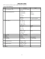
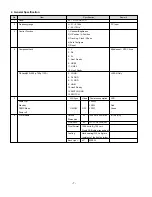
Summary of Contents for 37LB1D-UB

Page 1: ...RVICE MANUAL CAUTION BEFORE SERVICING THE CHASSIS READ THE SAFETY PRECAUTIONS IN THIS MANUAL CHASSIS LA61A MODEL 42LB1DR UA 42LB1DRA UA website http biz LGservice com e mail http www LGEservice com techsup html ...

Page 2: ...CT SAFETY 3 SPECIFICATION 6 ADJUSTMENT INSTRUCTION 11 SVC REMOCON 17 VIDEO TROUBLE SHOOTING BLOCK DIAGRAM 18 AUDIO TROUBLE SHOOTING BLOCK DIAGRAM 41 EXPLODED VIEW 53 EXPLODED VIEW PARTS LIST 54 REPLACEMENT PARTS LIST 55 SVC SHEET ...

Page 3: ...Current Cold Check Antenna Cold Check With the instrument AC plug removed from AC source connect an electrical jumper across the two AC plug prongs Place the AC switch in the on position connect one lead of ohm meter to the AC plug prongs tied together and touch other ohm meter lead in turn to each exposed metallic parts such as antenna terminals phone jacks etc If the exposed metallic part has a ...

Page 4: ...vely obtain and wear a commercially available discharging wrist strap device which should be removed to prevent potential shock reasons prior to applying power to the unit under test 2 After removing an electrical assembly equipped with ES devices place the assembly on a conductive surface such as aluminum foil to prevent electrostatic charge buildup or exposure of the assembly 3 Use only a ground...

Page 5: ...not shiny reheat them and if necessary apply additional solder Fuse and Conventional Resistor Removal Replacement 1 Clip each fuse or resistor lead at top of the circuit board hollow stake 2 Securely crimp the leads of replacement component around notch at stake top 3 Solder the connections CAUTION Maintain original spacing between the replaced component and adjacent components and the circuit boa...

Page 6: ...6 PAL N M 6 7 South America Market 7 NTSC M 7 Except South America NTSC Market ME 3 RF Input Channel VHF E2 E12 PAL UHF E21 E69 CATV S1 S20 HYPER S21 S47 L L B C D FRANCE VHF 2 13 NTSC UHF 14 69 CATV 1 125 VHF Low 1 M10 JAPAN VHF High 4 S22 UHF S23 62 4 Input Voltage AC 100 240 V 50Hz 60Hz 5 Market Worldwide 6 Picture Size 1067 308mm 42 02inch 42LB1R 7 Tuning System FVS 100 program PAL 200 PR Opti...

Page 7: ...9 LINE2 11 LINE3 13 Line3 Ready D4 Jack 525i 525p 750p 1125i 2 Y GND JAPAN Only 4 Pb GND 6 Pr GND 8 LINE1 10 Line2 Ready 12 SWITCH GND 14 SWITCH 5 H V Sync Video Power consumption LED Power ON 240W Stand by 3 0W Red DPMS Mode ON OFF OFF 30W Green Power off 6 LCD Module Outline 42 1006 x 610 x 56 mm H x V x D Dimension Pixel Pitch 42 0 227 x 0 681 x RGB mm Pixel Format 1366 horiz By 768 vert Pixels...

Page 8: ...5 Line ZE TE ME 5 720x576 31 25 50 00 HDTV 576p TE ME 6 1280x720 45 00 60 00 HDTV 720p TE ME 7 1280x720 44 96 59 94 HDTV 720p TE ME 8 1920x1080 31 25 50 00 HDTV 1080i 50Hz AU Ver TE ME 9 1920x1080 33 75 60 00 HDTV 1080i 60Hz ATSC TE ME 10 1920x1080 33 72 59 94 HDTV 1080i 59 94Hz TE ME 5 RGB PC INPUT Mode Table No Resolution H freq kHz V freq Hz Pixel clock MHz Proposed Analog RGB Digital RGB 1 720...

Page 9: ... HDMI DTV INPUT Mode Table 7 HDMI PC INPUT Mode Table No Resolution H freq kHz V freq Hz Pixel clock MHz Proposed Analog RGB Digital RGB 1 720x400 31 468 70 8 28 321 2 640x480 31 469 59 94 25 17 VESA 37 684 75 00 31 5 VESA 3 800x600 37 879 60 31 40 00 VESA 46 875 75 49 5 VESA 4 832x624 49 725 74 55 57 283 5 1024x768 48 363 60 00 65 00 VESA XGA 56 47 70 00 75 00 VESA XGA 60 123 75 029 78 75 VESA XG...

Page 10: ...osite 75 17 Ground Video input Output 18 Ground RGB Switching Control 19 Video output Composite 1V including sync 75 20 Video input Composite 1V including sync 75 21 Common ground Shield Table 2 Scart Arrangement 2 Half Scart Pin Signal Signal Level Impedance 1 Audio Output B right 0 5 Vrms 1 2 Audio Input B right 0 5 Vrms 10 3 Audio Output A left 0 5 Vrms 1 4 Ground audio 5 Ground blue 6 Audio in...

Page 11: ...his state Full White Pattern is displayed but you must preset the program for Full White State when you press the Main Power Off On 2 Pattern Mode is deselected by pressing CH Exit Key Set is activated HEAT RUN without signal generator in this mode 3 EPLD Download 1 Test Equipment PC Jig for download 2 Connect the power of VSC B D 3 Execute download program iMPACK of PC 4 After executing the hot k...

Page 12: ...on the Output window and the Download process is ended 8 The execution of process 6 is convenient when using the short cut icon 5 POD Certificate Download 5 1 Preparation for Adjustment 1 Connect the MEMORY JIG and PC 2 Turn on the JIG MAIN POWER SWITCH 3 After turn on the PC and MONITOR execute the Certificate Downloader v1 4 from the screen 5 2 Adjustment Sequence 1 After open the Certificate Do...

Page 13: ...Test Equipment 1 PC with Factory Test Program 2 VBI Inserter Norpak TES3 Guide Data Discharge Equipment In case of without the VBI Inserter TES3 a VCR may be used 6 2 Preparation for Adjustments 1 In case of with VBI Inserter TES3 Signal uses Cable input and set as below 2 In case of without VBI Inserter TES3 VCR uses Cable input and set as below Factory Test S W must be set to GlinkTo PC Card ON ...

Page 14: ...ID data write read 3 D Sub cable 4 Jig for HDMI Cable connection 2 Preparation for Adjustments Setting of Device 1 Set devices as below and turn on the PC and JIG 2 Open S W for writing DDC EDID data write read operated in DOS mode 14 Name Descrambler Check CableCARD OOB Path FDC_SNR Video Signal Normal OK CableCARDTM is inserted OK Lock OK 20dB above Normal Screen Defective Not OK CableCARDTM is ...

Page 15: ...TV31Bar in 1080i Mode and select Normal in screen 2 After receiving signal for at least 1 second press the ADJ Key on the Service R C to enter the Ez Adjust and select the 5 ADC 480p Comp2 RGB Pressing the Enter Key to adjust with automatic movement 3 When the adjustment is over ADC Component2 Success is displayed If the adjustment has errors ADC Configuration Error is displayed 4 After the Compon...

Page 16: ...mperature 9300 K 1000 K dUV 3dUV Warm X 0 314 0 015 Y 0 318 0 015 Color temperature 6500 K 1000 K dUV 3dUV 12 Video uPD Set Adjustment for reduce color difference Main Sub screen of RF or Video signal 12 1 Adjustment 1 Connection the Video Signal Generator Master to the TV AV Input terminal After input pattern Model 201 NTSC M Pattern 32 100 color Bar pressing the Rev button and appear as below fi...

Page 17: ...k the front AV To move channel up down or to select a function displayed on the screen To adjust the volume or accurately control a specific function To set a specific function or complete setting To move the channel down in the PIP screen To use as a red key in the teletext mode To move the channel in the PIP screen To use as a green key in the teletext mode To switch between the main and sub scr...

Page 18: ...UFFER MC33078 MST33611_HDMI IIC 1 0XC2 IIC 1 0XC0 IIC 2 0xB8 IIC 2 0xBA IIC 2 0x9C IIC 3 0x1C IIC 1 0xA6 IIC2 0x1E IIC 4 0x6C IIC 2 0x9C IIC 4 0x90 2 11 IIC 2 IIC 3 IIC 4 M_MSP 4440 SIF IIC 4 0x84 Video SW CXA2181 EPF_RGB PC RGBHV 5 IN1 AT NT_M_Tuner Main Sound Proc MSP4440 IIC 4 0x80 Sub MSP 4458G AT NT Tuner Rear L R Side L R I2S Main Sub PDR 656 0 7 1394_OUT_TP 0 7 1394_IN_TP 0 7 PVRsoc LGDT130...

Page 19: ... 19 VSB POD HD2 4 PVRSoc 656data MUX CPLD TP_OUT TP D1 QAM_TP VSB_TP SUB UPD TP_IN1 2 656 Digital B D MUX Interface ...

Page 20: ...1U PQ05DZ1U HDD HDD 5V_ST 5V_ST 3 3V_ST 3 3V_ST 242LP 242LP AZ1117 1 8 AZ1117 1 8 SC2595 SC2595 AZ1086 1 8 AZ1086 1 8 AZ1117 1 5 AZ1117 1 5 uPD64015 2 uPD64015 2 HY57161610 2 HY57161610 2 AZ1117 1 8 AZ1117 1 8 LGDT3703 LGDT3703 AZ1117 1 8 AZ1117 1 8 LGDT3703 LGDT3703 AT NT Tuner AT NT Tuner AT NT Tuner w OOB AT NT Tuner w OOB Ethernet BD Ethernet BD EPF Module EPF Module DDR RAM IC101 IC201 LCX244...

Page 21: ...V_ST 3 3V_ST 3 3V_ST SC1565 1 8 SC1565 1 8 IC504 5VST_RFSW 9 0V IC301 Si3865 Si3865 Si3865 Si3865 PWR_SW2 PWR_SW1 PQ05DZ1U PQ05DZ1U IC301 CXA2181 CXA2181 6V 6V 5 0V TAS5122 TAS5122 20V 20V NSP2100A NSP2100A AT24C16 AT24C16 IC502 200mA 3mA 163mA 28mA MSP4458G MSP4458G 145mA 25mA 24mA 5mA 3 3V 72mA 24mA BA033 3 3 BA033 3 3 1A 88mA Digital B D Power Block ...

Page 22: ...XA2069Q 0x90 U Com MTV412MF 0x50 CPU_I2C AT NT OOB Tuner TDVM H751P 0xC0 IEP2 LGDP4411 0x1E AV Switch CXA2181Q 0x84 DASP NSP2100A 0x6C CPLD EPM570 I2C_HUB _EN 1 4 DPLL LGDT1901B 0x12 PDP Module 0x1C Main VSB QAM LGDT3703B 0x1C Port Exp M62320 0x74 Temper Sensor DS1621 0x94 1080P De Inter FLI8668 0x76 0x78 Index Port Exp M62320 0x70 Sub MSP MSP4440K 0x88 NT Tuner Korea only TDVS H901P 0xC2 I2C_CH2 ...

Page 23: ...P D1 Gemstar Block Gemstar Block DDR 32MB DDR 32MB 656 TP In2 TP In1 SiI3512 SiI3512 Peri Bus PCI Bus PCI Bus PCI Bus TP Out11 VSB TP QAM TP TP Out2 CCIR656 V Q TP VSB TP QAM TP 1394 Out V Q TP Peri Bus TP Out12 656 TP In2 TP In1 1394 TP_In IEP3 IEP3 HD 2 4 TP De Mux MPEG Decoding MP HL Format Converter Host I F Memory I F Digital I F NTSC Encoder AC 3 Decoder SPDIF In out Video Pre proc Motion Es...

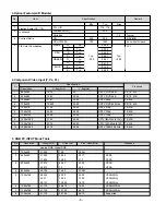
Page 24: ... 24 DCR DVR NO OSD ...

Page 25: ...heck L VDS Cable Check P DP Module Control bo ard 1 2 3 4 5 6 1 _Check the D1601 D1602 D1603 D1604 Digital board ON _Check Power c onnector Y Y Y Y Y Y N N Y N N 2 _Check the LGDP4412 IC804 inpu t signal Vsync DE Clk 33 75KHz 80 1MHz Hsync 33 75KHz 59 94Hz 3 _Check t he THC63LVD103 IC1302 input sign al _Sign al sh ape is same above 4 _Ch eck th e P801 input sig nal 27 DISP_EN 9 TXCC 80 1MHz 3 3V G...

Page 26: ... 26 DCR DVR RF AV MODE ...

Page 27: ...Check 74 FCT244 1Y1 3Y2 Sub Picture 1 _Check Anten na cable RF Switch Tuner 2 _Execu te DW or PIP 3 _Check Tun ers Vcc and Video out 4 _Check CXA2069 power inpu t signa l _TV V5 si gnal shape looks like figure7 1 5 _Check FMS6400 power inpu t signa l _Yin si gnal sh ape looks like figure7 1 6 _Check uPD64001 power input signal _AYI1 signal shape looks like figure7 1 7 _Check uPD64011 output signal...

Page 28: ...on TV DTV mo de Is it 5V 6 ou tp ut of TUNER TU1302 Is it 33V 8 o utp ut of TUNER TU1302 Is norma l 16 outp ut of TUNER TU1302 Replace th e TUNER TU1302 Is it 5V 12 ou tp ut of TUNER TU1302 Is it 33V 9 o utp ut ofTUNER TU1302 Is n ormal 16 o utput of TUNER TU1302 Replace th e TUNER TU1302 NO YES NO YES YES YES YES YES TV CATV mode does not display DCR RF MODE Detailed ...

Page 29: ...4 o utput of CXA2069 IC101 FIG1 Is n ormal o utpu of FMS6400 IC702 FIG2 Is n ormal UPD640 15 Power 1 5V 3 3V Is n oramlly co nnected P101 to P1612 Flat cab le Is nora ml out put of UPD64015 IC701 Digita l Output Y 10bit C 10bit H V FID FIG1 FIG2 TV CATV mode does not display Is n ormal o utpu of FMS6400 IC704 FIG2 Is n ormal UPD640 15 Power 1 5V 3 3V Is nora ml out put of UPD64015 IC701 Digita l O...

Page 30: ... 30 Component RGB HDMI DVI ...

Page 31: ...IC203 REF 1 CLKA4 15 8 Digit al Bo ard AV Board 7 _Check the MST3361 IC603 Output Signals Vsync DE Clk Hsync 59 94Hz Frequenc y Different acc ordi ng to form at Data 8 _Check CPLD IC301 HD 96 VD 95 6 _Check MS T3361 IC603 Power pins Input Signals Signa l Shape is S ame abo ve 9 _Check CY2309 IC203 REF 1 CLKA4 15 _Sig nal sh ape is same abo ve 1 _Check supported format ref owner s manual 2 _Check C...

Page 32: ... PLD IC301 V Sync H Sync O utput 95 VD 96 HD 1 _Check HDCP Error _Retr y po wer off and on TV or S TB DVD _Check MST3361 IC603 HDCP IIC line 69 70 2 _Check EDID Download RX0C RX0C Frequenc y Different acc ordi ng to form at 4 _Check MST3361 IC603 Outp uts 5 _Check CPLD IC301 V Sync H Sync Output 95 VD 96 HD _Sig nal sh ape is same abo ve SCL SDA 3 _ MST3361 IC603 inputs RX1C RX1C Vsync DE Clk Hsyn...

Page 33: ... 33 DCR DVR DTV CADTV ...

Page 34: ...id Error Data NG Check C PLD IC305 Outputs CLK SOP Valid Error Data 3 _ Check LGD T3703 IC1305 inputs power pi ns Osc 25Mhz IF pin Signal 4 _ Check LGDT3703 IC1305 Outputs 5 _ In case of DTV Check CPLD IC305 Inpu ts CLK SOP Valid Error Data _ Signal Shape is same above 6 _ In case o f CADTV Check POD Contro lle r _ Signal Shape is same above 7 _Check CPLD IC305 Inputs CLK SOP Valid Er ror Dat a 8 ...

Page 35: ... Block Video Pre proc Motion Estimator MPEG 2 SD Video Enc EISC ROM MEM Int Timer Bus Master System Decoder De scramblers ATSC DIRECTV ARIB DVB OC Ch Input I F PVR Up Controller Video Feature Extractor PVR Down Controller ATAPI I F SDRAM I F Ch Output I F SC AES DSC AES NTSC PAL Decoder DMA PCI2 2 Audio Encoder SCI I F PLL DLL LGDT1304 PVR SOC IC908 DDR 32MB DDR 32MB 656 TP In2 TP In1 SiI3512 IC10...

Page 36: ...ck PVRSoc LGDT1304P IC908 1 Check HDD Power cable 1 5V 4 12V 2 Check HDD Signal cable SATA 3 Check SiI3512 IC1002 inputs Power pins Osc Check LED1000 blinking Check PCI bus 4 Check CPLD IC305 inputs Clock Sop Valid Error Data 8bit PVRSoc Memory Test Hardware test Menu 5 Check CPLD IC305 outputs Clock Sop Valid Error Data 8bit TPCLK TPSOP TPVALID nTPERR TPDATA 7 0 byte0 47h byte1 byte2 byte187 CLK ...

Page 37: ...d off LED R ed repeatedl y of its elf No video Check X1100 10MHz Norm al PIC18F1220 IC1103 Norm al YES NO Replace PIC18F1220 IC1103 and Re No Vid eo Check CPL D LED and Re download download Re download YES Power On Off repetition Automatically ...

Page 38: ...Check P1604 AC DETECT P1604 1 is 5V HIGH NO No NO NO Replace p ower board Norm al NO Replace Po wer board Norm al Check P1603 power Power lin es and GND sh ort Replace A V boa rd or digital bo ard NO NO Check A V bo ard Mic om Check A V bo ard Mic om YES YES Check Fa n wafers and c onn ector s Norm al Check Fa ns Fan P1606 upper sid e 50 1EA 42 No FAN Protect Mode ...

Page 39: ...or Dispatcher knows the new MAC ID and CableCARD ID to complete the installation The original card should be marked accordingly and returned for repair 6 Check the CableCARD menu options If the second CableCARD fails to bring up the User Interface screen the technician should refer to the diagnostic menus on the DCR for further troubleshooting The technician can pull up the User Interface screen m...

Page 40: ... as MMI screen and has relayed the information to the dispatcher but is still not receiving encrypted programming this programming may be protected through the use of copy protection directive Ensure that the information passed to dispatch is correct Relay again the Host ID CableCARD ID and Data ID Motorola only Dispatch will send a hit to the CableCARD once the information is checked and verified...

Page 41: ...t AV Compone nt 2 Compone nt 1 RGB Audi o Monitor Out Buffer MC33078 ADC CS5331A MUX CPLD EPM570F256 NT Tun er AT NT Tuner HD 2 PVR SOC LGDT1304P SiI 3512 Main LGDT3703 HDD HDMI MST3361 System CPLD EPM570T144 CS8415A SPDIF Out Optical SPDIF L R L R L R L R SIF SIF TP I2S I2S L R I2S TP I2S SPDIF AUDIO TROUBLESHOOTING BLOCK DIAGRAM Audio Path ...

Page 42: ... 42 Common sound out ...

Page 43: ...rocess or MSP4450K PWM Modulator NSP2100A AMP TAS5122 Front Speaker Monitor Out Buffer MC33078 ADC CS5331A NT Tun er AT NT Tuner HD 2 System CPLD EPM570T144 SPDIF Out Optical SIF SIF I2S L R I2S I2S SPDIF TV RF NO Sound ...

Page 44: ... MCLK Check LG DT1102F IC402 inputs R413 LRCH R414 LRCK R415 SCK Fol lo w the pr ocedur e of COMMON SOUND OUT 7 8 Check N TSC Tuner TU1302 4 33V 7 18 5V 16 SIF Check An tenna Cable Check M C33078 IC1001 in outpu ts Power 8 9V 2 6 in pu t 1 7 output 9 4 MCLK 12 288MHz 3 LRCK 48KHz 1 LRCH Not 0 Volt age Level 36 SCI_R 37 SCI_L Not 0 Vol tage Level Analog si gnal Check C onnecto r P103 16 18 10 TV RF...

Page 45: ...Main Audi o Process or MSP4450K PWM Modulator NSP2100A AMP TAS5122 Front Speaker Monitor Out MUX CPLD EPM570F256 AT NT Tuner HD 2 Main LGDT3703 System CPLD EPM570 SPDIF Out Optical I2S TP SPDIF DTV NO Sound ...

Page 46: ...3 IC1305 outputs 44 45 47 49 50 52 54 55 VSB_DATA 57 ERROR 59 VALID 61 SOP 62 CLK 1 2 3 4 5 6 Check LG DT1102F IC402 7 Check AT NT Tuner TU1300 3 11 5V 24 IF_N 25 IF_P Check An tenna Cable Check M ux CPLD IC305 Fol lo w the pr ocedur e of COMMON SOUND OUT DTV NO Sound ...

Page 47: ... NSP2100A AMP TAS5122 Front Speaker AV AV Switch CXA2069 Front AV Compone nt 2 Compone nt 1 RGB Audi o Monitor Out Buffer MC33078 ADC CS5331A HD 2 System CPLD EPM570T144 SPDIF Out Optical L R L R L R L R I2S L R I2S I2S SPDIF AV Component RGB NO Sound ...

Page 48: ...C202 inputs 53 COMP1_L 54 COMP1_R 50 COMP2_L 51 COMP2_R 47 RGB_L 48 RGB_R Check M SP4450K IC202 outpu ts 36 SC1_R 37 SC1_L 4 5 Check C S5331 IC1000 in outputs Power 7 5V 5 8 L R input 1 LRCH 2 SCK 3 LRCK 4 MCLK Check LG DT1102F IC402 inputs R413 LRCH R414 LRCK R415 SCK Fol lo w the pr ocedur e of COMMON SOUND OUT 6 7 Check M C33078 IC1001 in outpu ts Power 8 9V 2 6 in pu t 1 7 output 8 Check C onn...

Page 49: ... 49 Main Audi o Process or MSP4450K PWM Modulator NSP2100A AMP TAS5122 Front Speaker Monitor Out HD 2 HDMI MST3361 System CPLD EPM570T144 CS8415A SPDIF Out Optical SPDIF I2S SPDIF HDMI NO Sound ...

Page 50: ...4 Check C S8415A IC1006 in outpu ts 14 HDMI_SPDIF 16 SCK 17 LRCK 18 SPDIF_OUT 10 SPDIF_CLK 5 SPDIF BYPASS Check MST3361 IC603 outputs 125 HDMI_SPDIF_OUT Fol lo w the pr ocedur e of COMMON SOUND OUT Check EP M570T144 IC301 Check SP DIF ou t R1035 HDMI NO Sound ...

Page 51: ...lator NSP2100A AMP TAS5122 Front Speaker AV Front AV Monitor Out Buffer MC33078 ADC CS5331A MUX CPLD EPM570F256 NT Tun er AT NT Tuner HD 2 PVR SOC LGDT1304P SiI 3512 Main LGDT3703 HDD System CPLD EPM570T144 SPDIF Out Optical TP I2S I2S L R I2S TP I2S SPDIF Record Play No Sound ...

Page 52: ...bits PCI Control si gn als Check siI3512 IC1002 inputs 14 B 15 B 19 A 20 A Check PP C405GPr IC100 in ou tputs PCI_AD 32 bits PCI Control si gn als PER_ADDR 32 bits PER_DATA 12 bit s PER Control si gna ls 4 5 Fol lo w the pr ocedur e of COMMON SOUND OUT Record Play No Sound ...

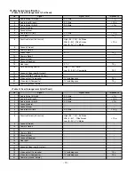
Page 53: ... 53 EXPLODED VIEW 010 051 052 020 060 070 120 110 040 090 100 130 140 080 030 ...

Page 54: ...mbly FRAME 42LB1DR A C SKD COST UP 68719ST936A PCB Assembly Sub T T LA61A SUB 42LB1DRA ALUSLLX SIDE A V BOARD TOTAL 49519K0115A Plate Assembly SHIELD MAIN DIGITAL 42LB1DRA UA 49519K0115H Plate Assembly SHIELD MAIN DIGITAL 42LB1DR A UA C SKD 68719ST937A PCB Assembly Sub T T LA61A SUB 42LB1DRA ALUSLLX CONTROL KEY BOARD TOTAL 68719ST937B PCB Assembly Sub T T LA61A SUB 42LB1DRA ALUSLLX CONTROL KEY FOR...

Page 55: ...22M 22u 20 16V C481 0CE476WF6DC MVK6 3TP16VC47M 47u 20 16V C482 0CE476WF6DC MVK6 3TP16VC47M 47u 20 16V C528 0CE106WFKDC MVK4 0TP16VC10M 10u 20 16V C531 0CE226WF6DC MVK5 0TP16VC22M 22u 20 16V C534 0CE226WF6DC MVK5 0TP16VC22M 22u 20 16V C601 0CE106WFKDC MVK4 0TP16VC10M 10u 20 16V C608 0CE106WFKDC MVK4 0TP16VC10M 10u 20 16V C613 0CE106WFKDC MVK4 0TP16VC10M 10u 20 16V C617 0CE106WFKDC MVK4 0TP16VC10M ...

Page 56: ...00CT 100n 10 50V C1301 0CC180CK41A C1608C0G1H180JT 18p 5 50V C1302 0CK103CK56A 0603B103K500CT 10n 10 50V DATE 2006 02 20 S AL LOC NO PART NO DESCRIPTION SPECIFICATION C1305 0CK104CK56A 0603B104K500CT 100n 10 50V C1306 0CK103CK56A 0603B103K500CT 10n 10 50V C1307 0CK105DF64A 0805F105Z160CT 1u 20TO 80 C1309 0CK105DF64A 0805F105Z160CT 1u 20TO 80 C1310 0CK103CK56A 0603B103K500CT 10n 10 50V C1311 0CK105...

Page 57: ...CK56A 0603B104K500CT 100n 10 50V C335 0CK104CK56A 0603B104K500CT 100n 10 50V C336 0CK104CK56A 0603B104K500CT 100n 10 50V DATE 2006 02 20 S AL LOC NO PART NO DESCRIPTION SPECIFICATION C337 0CK104CK56A 0603B104K500CT 100n 10 50V C338 0CK104CK56A 0603B104K500CT 100n 10 50V C339 0CK104CK56A 0603B104K500CT 100n 10 50V C340 0CK104CK56A 0603B104K500CT 100n 10 50V C341 0CK104CK56A 0603B104K500CT 100n 10 5...

Page 58: ...A C1608C0G1H220JT 22p 5 50V C660 0CK104CK56A 0603B104K500CT 100n 10 50V DATE 2006 02 20 S AL LOC NO PART NO DESCRIPTION SPECIFICATION C661 0CK104CK56A 0603B104K500CT 100n 10 50V C662 0CK104CK56A 0603B104K500CT 100n 10 50V C669 0CK104CK56A 0603B104K500CT 100n 10 50V C670 0CK104CK56A 0603B104K500CT 100n 10 50V C671 0CK104CK56A 0603B104K500CT 100n 10 50V C7004 0CK104CK56A 0603B104K500CT 100n 10 50V C...

Page 59: ...50V C858 0CK104CK56A 0603B104K500CT 100n 10 50V C859 0CK104CK56A 0603B104K500CT 100n 10 50V DATE 2006 02 20 S AL LOC NO PART NO DESCRIPTION SPECIFICATION C860 0CK104CK56A 0603B104K500CT 100n 10 50V C861 0CK104CK56A 0603B104K500CT 100n 10 50V C862 0CK104CK56A 0603B104K500CT 100n 10 50V C863 0CK104CK56A 0603B104K500CT 100n 10 50V C864 0CK104CK56A 0603B104K500CT 100n 10 50V C865 0CK104CK56A 0603B104K...

Page 60: ...00CT 100n 10 50V C1392 0CK105DF64A 0805F105Z160CT 1u 20TO 80 C1395 0CK104CK56A 0603B104K500CT 100n 10 50V DATE 2006 02 20 S AL LOC NO PART NO DESCRIPTION SPECIFICATION C1396 0CK104CK56A 0603B104K500CT 100n 10 50V C1618 0CK102CK56A 0603B102K500CT 1n 10 50V X C1621 0CK104CK56A 0603B104K500CT 100n 10 50V C1625 0CK102CK56A 0603B102K500CT 1n 10 50V X C1626 0CK102CK56A 0603B102K500CT 1n 10 50V X C1628 0...

Page 61: ...38A FSA1156P6X NL 1 65TO5 5V 40 IC203 0IMCRCY002A CY2309SC 1HT 3TO3 6V IC210 0IMCRCY002A CY2309SC 1HT 3TO3 6V IC504 0IMCRCY002A CY2309SC 1HT 3TO3 6V IC100 0IPRPBM001B PPC405GPR 3JB266C 1 7TO1 9V IC1002 0IMCR02015A SII3512ECTU128 1 71TO1 89V IC1101 0ISTL00024A MC14053BDR2G 3TO18V 0 02mA IC1202 0IMCRFA013A 74LCX244MTC 2TO3 6V 0 01mA IC303 0IMCRFA013A 74LCX244MTC 2TO3 6V 0 01mA IC306 0ISTLPH026A 74LV...

Page 62: ...013 HB 1M1608 121JT 120OHM 1 6X R1661 6210TCE0013 HB 1M1608 121JT 120OHM 1 6X R203 6210TCE0013 HB 1M1608 121JT 120OHM 1 6X R204 6210TCE0013 HB 1M1608 121JT 120OHM 1 6X DATE 2006 02 20 S AL LOC NO PART NO DESCRIPTION SPECIFICATION R244 6210TCE0013 HB 1M1608 121JT 120OHM 1 6X L1000 0LCML00020B MLI 201209 6R8K 6 8UH 10 L1001 0LCML00020B MLI 201209 6R8K 6 8UH 10 L1003 0LCML00020C MLI 201212 100K 10UH ...

Page 63: ...51R0 51OHM 5 1 16W R1302 0RD0331H609 RD 92T1J3R30 3300MOHM 5 1 R1634 0RD0332H609 RD 92T1J33R0 33OHM 5 1 2W DATE 2006 02 20 S AL LOC NO PART NO DESCRIPTION SPECIFICATION R1009 0RJ4701D677 MCR03EZPJ472 4 7KOHM 5 1 1 R1010 0RJ4701D677 MCR03EZPJ472 4 7KOHM 5 1 1 R1011 0RJ4702D677 MCR03EZPJ473 47KOHM 5 1 10 R1012 0RJ4701D677 MCR03EZPJ472 4 7KOHM 5 1 1 R1013 0RJ4701D677 MCR03EZPJ472 4 7KOHM 5 1 1 R1014 ...

Page 64: ...77 MCR03EZPJ820 82OHM 5 1 10W R3003 0RJ0822D677 MCR03EZPJ820 82OHM 5 1 10W R3074 0RJ0000D677 MCR03EZPJ000 0OHM 5 1 10W DATE 2006 02 20 S AL LOC NO PART NO DESCRIPTION SPECIFICATION R3075 0RJ0000D677 MCR03EZPJ000 0OHM 5 1 10W R3079 0RJ4701D677 MCR03EZPJ472 4 7KOHM 5 1 1 R3080 0RJ0000D677 MCR03EZPJ000 0OHM 5 1 10W R3084 0RJ0000D677 MCR03EZPJ000 0OHM 5 1 10W R316 0RJ0222D677 MCR03EZPJ220 22OHM 5 1 10...

Page 65: ...J1000D677 MCR03EZPJ101 100OHM 5 1 10 R921 0RJ1001D677 MCR03EZPJ102 1KOHM 5 1 10W DATE 2006 02 20 S AL LOC NO PART NO DESCRIPTION SPECIFICATION R925 0RJ4701D677 MCR03EZPJ472 4 7KOHM 5 1 1 R926 0RJ1001D677 MCR03EZPJ102 1KOHM 5 1 10W R935 0RJ4701D677 MCR03EZPJ472 4 7KOHM 5 1 1 R938 0RJ4701D677 MCR03EZPJ472 4 7KOHM 5 1 1 R939 0RJ4701D677 MCR03EZPJ472 4 7KOHM 5 1 1 R945 0RJ4701D677 MCR03EZPJ472 4 7KOHM...

Page 66: ...M 5 1 10W R1380 0RJ2201D677 MCR03EZPJ222 2 2KOHM 5 1 1 R1382 0RJ3300D677 MCR03EZPJ331 330OHM 5 1 10 DATE 2006 02 20 S AL LOC NO PART NO DESCRIPTION SPECIFICATION R1384 0RJ0222D677 MCR03EZPJ220 22OHM 5 1 10W R1385 0RJ0222D677 MCR03EZPJ220 22OHM 5 1 10W R1397 0RJ0222D677 MCR03EZPJ220 22OHM 5 1 10W R1398 0RJ0222D677 MCR03EZPJ220 22OHM 5 1 10W R1399 0RJ0222D677 MCR03EZPJ220 22OHM 5 1 10W R141 0RJ1001D...

Page 67: ... 10W R372 0RJ0222D677 MCR03EZPJ220 22OHM 5 1 10W R373 0RJ0222D677 MCR03EZPJ220 22OHM 5 1 10W DATE 2006 02 20 S AL LOC NO PART NO DESCRIPTION SPECIFICATION R376 0RJ0222D677 MCR03EZPJ220 22OHM 5 1 10W R377 0RJ0222D677 MCR03EZPJ220 22OHM 5 1 10W R380 0RJ0222D677 MCR03EZPJ220 22OHM 5 1 10W R381 0RJ0222D677 MCR03EZPJ220 22OHM 5 1 10W R382 0RJ0222D677 MCR03EZPJ220 22OHM 5 1 10W R383 0RJ0222D677 MCR03EZP...

Page 68: ...OHM 5 1 10W R775 0RJ1000D677 MCR03EZPJ101 100OHM 5 1 10 R776 0RJ1000D677 MCR03EZPJ101 100OHM 5 1 10 DATE 2006 02 20 S AL LOC NO PART NO DESCRIPTION SPECIFICATION R777 0RJ1000D677 MCR03EZPJ101 100OHM 5 1 10 R778 0RJ1000D677 MCR03EZPJ101 100OHM 5 1 10 R779 0RJ1000D677 MCR03EZPJ101 100OHM 5 1 10 R780 0RJ1000D677 MCR03EZPJ101 100OHM 5 1 10 R814 0RJ0222D677 MCR03EZPJ220 22OHM 5 1 10W R815 0RJ0222D677 M...

Page 69: ...0TP50VC1M 1u 20 50V 5 C112 0CE225WK6DC MVK4 0TP50VC2 2M 2 2u 20 5 C115 0CE105WK6DC MVK4 0TP50VC1M 1u 20 50V 5 C116 0CE227WF6DC MVK8 0TP16VC220M 220u 20 1 C117 0CE227WF6DC MVK8 0TP16VC220M 220u 20 1 C121 0CE225WK6DC MVK4 0TP50VC2 2M 2 2u 20 5 C122 0CE225WK6DC MVK4 0TP50VC2 2M 2 2u 20 5 C126 0CE105WK6DC MVK4 0TP50VC1M 1u 20 50V 5 C127 0CE105WK6DC MVK4 0TP50VC1M 1u 20 50V 5 C203 0CE226WF6DC MVK5 0TP1...

Page 70: ...00CT 100n 10 50V C315 0CK104CK56A 0603B104K500CT 100n 10 50V C316 0CK334CF94A C1608Y5V1C334ZT 330n 20TO DATE 2006 02 20 S AL LOC NO PART NO DESCRIPTION SPECIFICATION C317 0CK104CK56A 0603B104K500CT 100n 10 50V C322 0CK104CK56A 0603B104K500CT 100n 10 50V C323 0CC102CK41A C1608C0G1H102JT 1n 5 50V C C325 0CK104CK56A 0603B104K500CT 100n 10 50V C326 0CK104CK56A 0603B104K500CT 100n 10 50V C329 0CK104CK5...

Page 71: ...20 SMD D101 0DSIH00028A MC2838 T112 1 1200MV 75V 30 D102 0DSIH00028A MC2838 T112 1 1200MV 75V 30 ZD109 0DZ560009DA UDZS5 6B 5600MV 5 49TO5 73V DATE 2006 02 20 S AL LOC NO PART NO DESCRIPTION SPECIFICATION ZD201 0DZRM00248A RLZ8 2B 8200MV 7 78TO8 19V ZD202 0DZRM00248A RLZ8 2B 8200MV 7 78TO8 19V ZD601 0DZ560009DA UDZS5 6B 5600MV 5 49TO5 73V ZD602 0DZ560009DA UDZS5 6B 5600MV 5 49TO5 73V ZD603 0DZ5600...

Page 72: ...T NO DESCRIPTION SPECIFICATION R150 0RJ0752D677 MCR03EZPJ750 75OHM 5 1 10W R155 0RJ0000D677 MCR03EZPJ000 0OHM 5 1 10W R157 0RJ1002D677 MCR03EZPJ103 10KOHM 5 1 10 R158 0RJ1001D677 MCR03EZPJ102 1KOHM 5 1 10W R159 0RJ4703D677 MCR03EZPJ474 470KOHM 5 1 1 R160 0RJ4703D677 MCR03EZPJ474 470KOHM 5 1 1 R161 0RJ4701D677 MCR03EZPJ472 4 7KOHM 5 1 1 R162 0RJ0000D677 MCR03EZPJ000 0OHM 5 1 10W R163 0RJ0000D677 MC...

Page 73: ...82OHM 5 1 10W R698 0RJ0822D677 MCR03EZPJ820 82OHM 5 1 10W R699 0RJ0822D677 MCR03EZPJ820 82OHM 5 1 10W DATE 2006 02 20 S AL LOC NO PART NO DESCRIPTION SPECIFICATION R102 0RJ5100D677 MCR03EZPJ511 510OHM 5 1 10 R104 0RJ5100D677 MCR03EZPJ511 510OHM 5 1 10 R105 0RJ1501D677 MCR03EZPJ152 1 5KOHM 5 1 1 R106 0RJ1000D677 MCR03EZPJ101 100OHM 5 1 10 R107 0RJ1501D677 MCR03EZPJ152 1 5KOHM 5 1 1 R108 0RJ9100D677...

Page 74: ...03EZPJ101 100OHM 5 1 10 R591 0RJ1000D677 MCR03EZPJ101 100OHM 5 1 10 R592 0RJ1000D677 MCR03EZPJ101 100OHM 5 1 10 R593 0RJ1000D677 MCR03EZPJ101 100OHM 5 1 10 R594 0RJ1001D677 MCR03EZPJ102 1KOHM 5 1 10W R595 0RJ1001D677 MCR03EZPJ102 1KOHM 5 1 10W R596 0RJ3302D677 MCR03EZPJ333 33KOHM 5 1 10 DATE 2006 02 20 S AL LOC NO PART NO DESCRIPTION SPECIFICATION R597 0RJ1000D677 MCR03EZPJ101 100OHM 5 1 10 R598 0...

Page 75: ...CR10EZHJ220 22OHM 5 1 8W R108 0RH0222D622 MCR10EZHJ220 22OHM 5 1 8W R109 0RH0222D622 MCR10EZHJ220 22OHM 5 1 8W R110 0RH0222D622 MCR10EZHJ220 22OHM 5 1 8W R111 0RH0222D622 MCR10EZHJ220 22OHM 5 1 8W R112 0RH0222D622 MCR10EZHJ220 22OHM 5 1 8W R115 0RH0222D622 MCR10EZHJ220 22OHM 5 1 8W R116 0RH1001D622 MCR10EZHJ102 1KOHM 5 1 8W R117 0RH4701D622 MCR10EZHJ472 4 7KOHM 5 1 8 R118 0RH1001D622 MCR10EZHJ102 ...

Page 76: ......

Page 77: ......

Page 78: ......

Page 79: ......

Page 80: ......

Page 81: ...Feb 2006 Printed in Korea P NO 38289S0043Y ...

Reviews: