background image

Vertical Block 

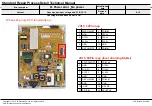
Source TAB IC Defect 

Horizontal Block 

Gate TAB IC Defect 

Gate TAB IC Defect 

Gate TAB IC Defect 

Vertical Line 

Source TAB IC Defect 

Vertical Block 

Source TAB IC Defect 

Horizontal Block 

Gate TAB IC Defect 

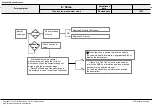
Horizontal line 

Gate TAB IC Defect 

Gate TAB IC Defect 

Horizontal Block 

Gate TAB IC Defect 

Appendix : Exchange the Module (2) 

Un-repairable Cases 

In this case please exchange the module. 

 A-5/5 

Copyright ⓒ 2015 LG Electronics. Inc. All right reserved. 
Only for training and service purposes

LGE Internal Use Only 

Summary of Contents for 40LF6300

Page 1: ...ODEL 40LF6300 40LF6300 UA CAUTION BEFORE SERVICING THE CHASSIS READ THE SAFETY PRECAUTIONS IN THIS MANUAL LED TV SERVICE MANUAL North Latin America http aic lgservice com Europe Africa http eic lgservice com Asia Oceania http biz lgservice com Internal Use Only ...

Page 2: ...t LG Electronics Inc All rights reserved Only for training and service purposes CONTENTS CONTENTS 2 PRODUCT SAFETY 3 SPECIFICATION 6 ADJUSTMENT INSTRUCTION 13 EXPLODED VIEW 22 SCHEMATIC CIRCUIT DIAGRAM APPENDIX TROUBLESHOOTING APPENDIX ...

Page 3: ...inals etc to be sure the set is safe to operate without damage of electrical shock Leakage Current Cold Check Antenna Cold Check With the instrument AC plug removed from AC source connect an electrical jumper across the two AC plug prongs Place the AC switch in the on position connect one lead of ohm meter to the AC plug prongs tied together and touch other ohm meter lead in turn to each exposed m...

Page 4: ...lectrostatic charge on your body by touching a known earth ground Alter natively obtain and wear a commercially available discharging wrist strap device which should be removed to prevent poten tial shock reasons prior to applying power to the unit under test 2 After removing an electrical assembly equipped with ES devices place the assembly on a conductive surface such as aluminum foil to prevent...

Page 5: ...he solder joints of the two original leads If they are not shiny reheat them and if necessary apply additional solder Fuse and Conventional Resistor Removal Replacement 1 Clip each fuse or resistor lead at top of the circuit board hollow stake 2 Securely crimp the leads of replacement component around notch at stake top 3 Solder the connections CAUTION Maintain original spacing between the replace...

Page 6: ...condition Each part is tested as below without special notice 1 Temperature 20 ºC 5 ºC 2 Relative Humidity 65 10 3 Power Voltage Standard input voltage 100 240V 50 60Hz 4 Specification and performance of each parts are followed each drawing and specification by part number in accordance with BOM 5 The receiver must be operated for about 20 minutes prior to the adjustment 3 Test method 1 Performanc...

Page 7: ...t Carbon Titan HEESUNG ELECTRON ICS LTD HEESUNG HC400DUN VCKN1 P N EAJ63088601 40LF6300 UA LC430EUE FHM1 FHD 43INCH 1920X1080 300CD COLOR 68 16 9 1200 1 60Hz Inverter N LED 2D TBD LG Display Co Ltd LGD LC430EUE FHM1 P N EAJ63109701 43LF6300 UA LC490EUE FHM1 FHD 49INCH 1920X1080 300CD COLOR 68 16 9 1200 1 60Hz Inverter N LED 2D With T con 51 1W 47W 4 1W 8Bit 10000K 178 178 GTGBW 9ms LVDS 2ch Car bo...

Page 8: ... 6 1280 720 44 96 59 94 74 176 HDTV 720P 7 1920 1080 33 75 60 00 74 25 HDTV 1080I 8 1920 1080 33 72 59 94 74 176 HDTV 1080I 9 1920 1080 67 50 60 148 50 HDTV 1080P 10 1920 1080 67 432 59 94 148 352 HDTV 1080P 5 2 Component 3D input Y CB PB CR PR No Resolution H freq kHz V freq kHz Pixel clock 3D input proposed mode Proposed 1 1280 720 45 00 60 00 74 25 2D to 3D Side by Side Top and Bottom HDTV 720P...

Page 9: ... WXGA X 8 1280 1024 63 981 60 020 108 00 VESA SXGA O 9 1920 1080 67 5 60 148 5 HDTV 1080P O DTV 1 640 480 31 469 59 94 25 175 SDTV 480P 2 640 480 31 5 60 25 200 SDTV 480P 3 720 480 31 50 60 27 027 SDTV 480P 4 720 480 31 469 59 94 27 00 SDTV 480P 5 1280 720 45 00 60 00 74 25 HDTV 720P 6 1280 720 44 96 59 94 74 176 HDTV 720P 7 1920 1080 33 75 60 00 74 25 HDTV 1080I 8 1920 1080 33 72 59 94 74 176 HDT...

Page 10: ... 29 97 30 00 74 175 74 25 S S T B S S Full 67 50 30 00 148 5 F P L A 60 00 S S T B 5 5 3D HDMI PC Input No Resolution H freq kHz V freq Hz Pixel clock MHz 3D input proposed mode 1 1024 768 48 363 60 004 65 000 2D to 3D S S T B 2 1360 768 47 712 60 015 85 500 3 1920 1080 67 50 60 00 148 50 2D to 3D S S T B C B R I C I 5 6 HDMI Input 1 3 No Resolution H freq kHz V freq Hz Pixel clock MHz 3D input pr...

Page 11: ...ide Top and Bottom HDTV 1080P 5 7 2 3D Manual Movie No Resolution H freq kHz V freq kHz 3D input proposed mode 1 Under 704 480 2D to 3D 2 Over 704 480i 2D to 3D Side by side Top and Bottom 3 Over 704 480p 50 60 2D to 3D Side by side Top and Bottom Checkerboard Row Interleaving Column Interleaving Frame Sequential 4 Over 704 480p Others 2D to 3D Side by side Top and Bottom Checkerboard Row Interlea...

Page 12: ... MHz Proposed 3D input proposed mode 1 1280 720 45 000 60 74 25 HDTV 720P 2D to 3D Side by Side Top Bottom 2 1920 1080 33 75 60 74 25 HDTV 1080I 2D to 3D Side by Side Top Bottom 5 9 2D to 3D Conversion RF 3D Input DTV No INPUT Freq Resolution 1 Digital TV Analog TV 2D Support freq 2D Support resolution 2 HDMI 2D Support freq 2D Support resolution 3 Component 2D Support freq 2D Support resolution 4...

Page 13: ...tern 09ch there can some afterimage in the black level area 3 Adjustment items 3 1 Main PCBA Adjustments 1 ADC adjustment OTP Component 2 EDID downloads for HDMI 3 2 Final assembly adjustment 1 White Balance adjustment 2 RS 232C functionality check 3 Factory Option setting per destination 4 Shipment mode setting In Stop 5 GND and HI POT test 3 3 Appendix 1 Tool option menu USB Download S W Update ...

Page 14: ... realization of Plug and Play 4 4 2 Equipment Since embedded EDID data is used EDID download JIG HDMI cable and D sub cable are not need Adjust remocon 4 4 3 EDID DATA 4 4 3 1 2D_8bit_PCM US _ xvYCC off HDMI EDID 2D_8bit_PCM US _xvYCC off Reference HDMI1 HDMI3 In the data of EDID bellows may be different by S W or Input mode ⓐ Product ID HEX EDID Table DDC Function 0001 0100 Analog 0001 0100 Digit...

Page 15: ... 67 03 0C 00 30 00 B8 2D 4 4 3 3 3D_8bit_PCM US _ xvYCC off HDMI EDID 3D_8bit_PCM US _xvYCC off Reference HDMI1 HDMI4 In the data of EDID bellows may be different by S W or Input mode ⓐ Product ID HEX EDID Table DDC Function 0001 0100 Analog 0001 0100 Digital ⓑ Serial No Controlled on production line ⓒ Month Year Controlled on production line ex Monthly 01 01 Year 2015 19 ⓓ Model Name Hex LGTV Cha...

Page 16: ...Objective How it works 1 Objective To reduce each Panel s W B deviation 2 How it works When R G B gain in the OSD is at 192 it means the panel is at its Full Dynamic Range In order to prevent saturation of Full Dynamic range and data one of R G B is fixed at 192 and the other two is lowered to find the desired value 3 Adj condition normal temperature Surrounding Temperature 25 5 C Warm up time Abo...

Page 17: ...ustment 1 Set TV in Adj mode using POWER ON 2 Zero Calibrate the probe of Color Analyzer then place it on the center of LCD module within 10cm of the surface 3 Press ADJ key EZ adjust using adj R C à 9 White Balance then press the cursor to the right KEY When KEY is pressed 206 Gray internal pattern will be displayed 4 Adjust Cool modes i Fix the one of R G B gain to 192 default data and decrease ...

Page 18: ...91 315 331 8 80 119 272 271 287 290 314 330 9 Over 120 271 270 286 289 313 329 3 O S Module AUO INX Sharp CSOT BOE cool med warm x y x y x y spec 271 270 286 289 313 329 target 278 280 293 299 320 339 5 2 Option selection per country 5 2 1 Overview 1 Tool option selection is only done for models in Non USA North America due to rating 2 Applied model LA42B Chassis applied to CANADA and MEXICO 5 2 2...

Page 19: ...ses 3D mode without 3D glasses Fig 2 Fig 3 OK in 3D mode without 3D glasses NG in 3D mode without 3D glasses 5 5 3 3D Inner pattern 1 Using RS232 Command Command Set ACK Transmission A I Set ID 72 Cr O K x or N G x 2 It support internal 3D pattern without MASTER equipment Except that one other method is same when use the MASTER equipment 5 6 HDMI ARC Function Inspection 5 6 1 Test equipment Optic ...

Page 20: ... No Item Min Typ Max Unit Remark 1 Audio practical max Output L R Distor tion 10 max Output 9 0 8 5 10 0 8 9 12 0 9 9 W Vrms 1 Measurement condition EQ AVL Clear Voice Off 2 Speaker 8Ω Impedance ALL MODEL 7 GND and HI POT Test 7 1 GND HI POT auto check preparation 1 Check the POWER CABLE and SIGNAL CABE insertion condition 7 2 GND HI POT auto check 1 Pallet moves in the station POWER CORD AV CORD ...

Page 21: ...rounding area surrounding lighting should be lower 10 lux Try to isolate adj area into dark surrounding 2 Probe location Color Analyzer CA 210 probe should be within 10cm and perpendicular of the module surface 80 100 3 Aging time After Aging Start Keep the Power ON status during 5 Minutes In case of LCD Back light on should be checked using no signal or Full white pattern 10 1 2 Equipment 1 Color...

Page 22: ...s These parts are identified by in the Schematic Diagram and EXPLODED VIEW It is essential that these special safety parts should be replaced with the same components as recommended in this manual to prevent Shock Fire or other Hazards Do not modify the original design without permission of manufacturer IMPORTANT SAFETY NOTICE 900 200 400 800 540 810 910 521 530 820 502 121 120 LV1 A10 Set Stand S...

Page 23: ..._NORMAL R174 200 1 3 3V_NORMAL R173 200 1 OPM1 SOC_RX AR100 33 1 16W C101 10pF C102 10pF 5V_NORMAL R11033 10K NON_CI R11034 10K NON_CI IC103 2 BR24G256FJ 3 NVRAM_ROHM 3 A2 2 A1 4 GND 1 A0 5 SDA 6 SCL 7 WP 8 VCC X101 24MHz 4 GND_2 1 X TAL_1 2 GND_1 3 X TAL_2 AR102 3 3K AR103 3 3K AR104 3 3K AR105 33 IC101 LG1311 C1 XIN_MAIN B23 XO_MAIN A23 PORES_N AG21 BOOT_MODE AJ18 PLLSET0 AB8 PLLSET1 AC8 OPM0 AD...

Page 24: ... NON_SS_DDR R231 4 7K R234 10K ODT_46_ohm MODEL_OPT_13 R233 10K ODT_55_ohm R239 10K OPT MODEL_OPT_15 R237 10K OPT MODEL_OPT_14 R240 10K OPT R236 10K R235 10K OPT MODEL_OPT_16 R238 10K TU_RESET2 IC101 LG1311 C1 TP_DVB_CLK AH30 TP_DVB_SOP AH32 TP_DVB_VAL AH31 TP_DVB_ERR AH33 TP_DVB_DATA7 AM33 TP_DVB_DATA6 AL32 TP_DVB_DATA5 AL33 TP_DVB_DATA4 AK32 TP_DVB_DATA3 AK33 TP_DVB_DATA2 AK31 TP_DVB_DATA1 AJ30 ...

Page 25: ...1 DDR3_OPT1 COMP1_Pb R370 0 GOOGLE SMARTCARD_RST SD_EMMC_DATA 2 R352 22K EU I2S_AMP SC_CVBS_IN_SOC C357 1uF 10V D1 _HDMI1 AUD_SCK D0 _HDMI1 R333 33 C313 4 7uF 10V COMP1_Y_IN_SOC SCART_LOUT_SOC R360 33 IF_N AUAD_R_CH3_IN CK _HDMI2 HP_ROUT_MAIN SMARTCARD_VCC SD_EMMC_CMD C339 100pF 50V OPT R385 4 7K OPT SMARTCARD_DET SD_EMMC_DATA 3 D1 _HDMI3 CK _HDMI3 D0 _HDMI3 D2 _HDMI3 D2 _HDMI3 CK _HDMI3 D0 _HDMI3...

Page 26: ...8 DQL6 G2 DQL7 H7 DQU0 D7 DQU1 C3 DQU2 C8 DQU3 C2 DQU4 A7 DQU5 A2 DQU6 B8 DQU7 A3 VREFCA M8 VREFDQ H1 ZQ L8 VDD_1 B2 VDD_2 D9 VDD_3 G7 VDD_4 K2 VDD_5 K8 VDD_6 N1 VDD_7 N9 VDD_8 R1 VDD_9 R9 VDDQ_1 A1 VDDQ_2 A8 VDDQ_3 C1 VDDQ_4 C9 VDDQ_5 D2 VDDQ_6 E9 VDDQ_7 F1 VDDQ_8 H2 VDDQ_9 H9 NC_1 J1 NC_2 J9 NC_3 L1 NC_4 L9 A14 T7 VSS_1 A9 VSS_2 B3 VSS_3 E1 VSS_4 G8 VSS_5 J2 VSS_6 J8 VSS_7 M1 VSS_8 M9 VSS_9 P1 V...

Page 27: ...M7 BA0 M2 BA1 N8 BA2 M3 CK J7 CK K7 CKE K9 CS L2 ODT K1 RAS J3 CAS K3 WE L3 RESET T2 DQSL F3 DQSL G3 DQSU C7 DQSU B7 DML E7 DMU D3 DQ0 E3 DQ1 F7 DQ2 F2 DQ3 F8 DQ4 H3 DQ5 H8 DQ6 G2 DQ7 H7 DQ8 D7 DQ9 C3 DQ10 C8 DQ11 C2 DQ12 A7 DQ13 A2 DQ14 B8 DQ15 A3 VREFCA M8 VREFDQ H1 ZQ L8 VDD_1 B2 VDD_2 D9 VDD_3 G7 VDD_4 K2 VDD_5 K8 VDD_6 N1 VDD_7 N9 VDD_8 R1 VDD_9 R9 VDDQ_1 A1 VDDQ_2 A8 VDDQ_3 C1 VDDQ_4 C9 VDDQ...

Page 28: ...2 W12 AVDD11_C4TX_3 Y12 AVDD11_C4TX_4 AA12 DVDD11_XTAL G18 DVDD11_DR3PLL H18 DVDD11_CVBSPLL AF23 AVDD11_DMD_1 AF24 AVDD11_DMD_2 AF25 DVDD18_EMMC_1 L26 DVDD18_EMMC_2 M26 IC101 LG1311 C1 GND_1 B22 GND_2 B24 GND_3 C22 GND_4 C23 GND_5 C24 GND_6 D4 GND_7 D5 GND_8 D6 GND_9 D20 GND_10 D21 GND_11 E6 GND_12 E20 GND_13 E21 GND_14 F6 GND_15 F7 GND_16 F8 GND_17 F18 GND_18 F19 GND_19 F20 GND_20 F21 GND_21 G7 G...

Page 29: ...4 22uF 10V C2354 10uF 10V R2319 430K 1 16W 1 R2339 10K C2300 22uF 10V R2312 10K INV_CTL C2339 10uF 10V C2346 22uF 10V C2303 0 1uF 25V 3 3V_EMMC PWM_DIM2 C2327 330pF 50V POWER_DET R2313 4 7 1 16W 5 R2307 100 PANEL_VCC 3 3V_NORMAL C2335 100pF 50V OPT L2308 C2319 0 1uF 16V R2342 10K R2346 3 3K LVDS_DISCHARGE R2320 560K 1 10W 5 13V VA23001 5 6V AMOTECH CO LTD Default_Amotech C2326 10uF 25V C2309 10uF ...

Page 30: ...20 SDA20 19 P13 TXD2 SO20 20 P12 SO00 TXD0 TOOLTXD 21 P11 SI00 RXD0 TOOLRXD SDA00 22 P10 SCK00 SCL00 23 P146 24 P147 ANI18 25 P27 ANI7 26 P26 ANI6 27 P25 ANI5 28 P24 ANI4 29 P23 ANI3 30 P22 ANI2 31 P21 ANI1 AVREFM 32 P20 ANI0 AVREFP 33 P130 34 P01 TO00 RXD1 35 P00 TI00 TXD1 36 P140 PCLBUZ0 INTP6 37 P120 ANI19 38 P41 TI07 TO07 39 P40 TOOL0 40 RESET 41 P124 XT2 EXCLKS 42 P123 XT1 43 P137 INTP0 44 P1...

Page 31: ..._SDA_4 R3276 14K MHL R3243 1K 1 16W 5 MHL SPDIF_OUT_ARC 3 3V_NORMAL R3202 330K MHL C3228 22uF 10V OPT D2 _HDMI2 R3204 100K MHL R3268 1K HDMI_EXT_EDID D1 _HDMI2 D2 _HDMI4 D2 _HDMI1 D3210 IP4294CZ10 TBR ESD_HDMI_TMDS 1 8 2 7 3 6 4 5 9 10 5V_HDMI_4 C3226 0 1uF 16V OPT Q3206 MMBT3904 NXP HDMI_EXT_EDID E B C VA3205 ESD_HDMI HDMI_HPD_2 D2 _HDMI1 D3205 A2 C A1 VA3206 ESD_HDMI DDC_SDA_4 C3227 0 1uF 16V D3...

Page 32: ..._OUT 3 3V_NORMAL R3409 100 HP_OUT C328 1000pF SPDIF_OUT DOUT1 VA3806 5 5V TP3400 C325 0 047uF JK3403 PEJ034 01 6B T_TERMINAL2 7B B_TERMINAL2 5 T_SPRING 4 R_SPRING 3 E_SPRING R3801 1K SOC_TX VA3800 5 6V Default_Amotech SOC_RX HP_LOUT COMP1_Pb VA3805 5 5V R3802 1K DOUT1 3 3V_NORMAL TP3401 VA3802 5 6V Default_Amotech R3806 10K VA3801 5 6V Default_Amotech P3400 12507WS 04L 1 2 3 4 5 R3827 10K OPT COMP...

Page 33: ...9 10K 5 C4009 0 1uF 16V OPT BT_RESET R4002 100 C4015 5pF 50V WIFI_DMDP_5pF D4000 RCLAMP0502BA OPT WIFI_DP 3 5V_ST C4002 0 1uF OPT KEY2 P4000 SMAW200 H18S5 14 KEY2 9 SDA 4 USB_DM 18 GND 13 GND 8 GND 3 BT_RESET 17 LED_R 12 KEY1 7 WOL 2 3 5V_WIFI 16 3 5V_ST 11 SCL 6 USB_DP 1 GND 15 IR 10 GND 5 NC 19 GND R4020 2K IC4001 AP2191WG 7 3 FLG 2 GND 4 EN 1 OUT 5 IN 3 5V_ST R4021 33 R4022 10K OPT WIFI_EN C401...

Page 34: ...5 USB_DM3 D4303 5V USB_ESD_SD05 5V_USB_3 USB_DP3 USB_DP2 JK4300 3AU04S 305 ZC LG 1 2 3 4 5 C4323 22uF 10V C4311 22uF 10V C4322 10uF 10V C4310 10uF 10V D4302 RCLAMP0582B USB_ESD_0582B D4300 RCLAMP0582B USB_ESD_0582B D4302 1 RCLAMP0502BA USB_ESD_0502BA D4300 1 RCLAMP0502BA USB_ESD_0502BA D4302 2 DF3D6 8MS Multi_Toshiba D4300 2 DF3D6 8MS Multi_Toshiba MID_LG1311 1 2014 05 28 USB 2 3 PAGE 13 MAX 1 5A ...

Page 35: ... 16V 5V_NORMAL USB_CTL1 USB_OCD1 JK4500 3AU04S 305 ZC LG 1 2 3 4 5 D4501 5V USB_ESD_SD05 C4502 22uF 10V OPT R4502 14K 1 IC4500 BD2242G 3 EN 2 GND 4 OC 1 VIN 6 VOUT 5 ILIM R4501 4 7K C4501 10uF 10V D4500 RCLAMP0582B USB_ESD_0582B D4500 1 RCLAMP0502BA USB_ESD_0502BA D4500 2 DF3D6 8MS Multi_Toshiba 1 MID_LG1311 USB 1 DVR 2014 05 28 PAGE 14 USB1 2 0 MAX 1 5A OCP USB1 value change 10K 2 63V 4 7K 2 97V ...

Page 36: ...TS BE USED FOR THE CRITICAL COMPONENTS IN THE SYMBOL MARK OF THE SCHEMETIC C5000 0 1uF 16V D5002 5 5V LAN_ESD D5001 5 5V LAN_ESD C5001 0 01uF 50V JK5000 RJ45VT 01SN002 1 1 2 2 3 3 4 4 5 5 6 6 7 7 8 8 9 9 D5000 5 5V LAN_ESD EPHY_RDN EPHY_RDP EPHY_TDN EPHY_TDP D5003 5 5V LAN_ESD PAGE 16 Ethernet Block Copyright ⓒ 2015 LG Electronics Inc All right reserved Only for training and service purposes LGE I...

Page 37: ...10OUT 30 AVDD33_2 31 CKXTAL1 32 CKXTAL2 5 MDI 1 8 RXDV 6 MDI 1 4 MDI 0 2 AVDD10OUT 33 EP R5204 2 49K 1 C5200 4 7uF 10V ET_COL SNI R5200 3 3K R5202 1M OPT LAN_JACK_POWER C5208 0 1uF 16V C5211 0 1uF 16V ET_COL SNI EPHY_TDP EPHY_ACTIVITY EPHY_RXD0 EPHY_RDP 3 5V_WOL EPHY_RXD1 EPHY_CRS_DV R5217 3 3K EPHY_TXD1 EPHY_MDC C5204 0 1uF C5209 33pF EPHY_TXD0 R5210 33 R5209 51 C5201 0 1uF 16V R5223 33 IC5201 AP...

Page 38: ...P 3 3V_NORMAL C5605 22000pF 50V AMP_RESET_N POWER_DET R5601 10K AMP_MUTE_MICOM AUD_LRCH I2C_SDA1 L5602 NRS6045T100MMGK 10 0uH R5608 4 7K C5610 1uF 10V C5608 22000pF 50V C5617 0 47uF 50V R5603 3 3 1 10W C5612 390pF 50V 3 3V_NORMAL L5605 NRS6045T100MMGK 10 0uH 13V_AMP SPK_L 10uF C5607 25V SPK_L AMP_MUTE SPK_R R5690 100 AMP_MUTE_PWR_DET L5604 NRS6045T100MMGK 10 0uH SPK_R L5600 UBW2012 121F L5601 BLM1...

Page 39: ...UT 3 OUTR 2 INR 4 GND_1 1 INR 6 VSS 5 MUTE 7 CN 8 CP 9 VDD 10 GND_2 11 UVP 12 OUTL 13 INL 14 INL R6106 43K 1 HP_OUT R6101 10K HP_OUT C6102 1uF 10V HP_OUT R6103 43K 1 HP_OUT C6104 18pF HP_OUT C6101 1uF 10V HP_OUT R6105 4 7K HP_OUT 3 3V_NORMAL R6102 43K 1 HP_OUT C6109 18pF HP_OUT C6105 1uF 10V HP_OUT C6103 1uF 10V HP_OUT SIDE_HP_MUTE C6108 10pF 50V HP_OUT R6100 10K HP_OUT C6107 0 1uF 16V HP_OUT 3 3V...

Page 40: ...RF 12 ERROR 13 GND_1 14 MCLK 15 SYNC 16 VALID 17 DATA 18 NC_3 19 NC_4 20 NC_5 21 NC_6 22 NC_7 23 NC_8 24 NC_9 25 RESET_DEMOD 26 3 3V_DEMOD 27 SCL_DEMOD 28 1 2V_DEMOD 29 NC_10 30 SDA_DEMOD 47 SHIELD B1 B1 A1 A1 R6401 1 0 TU_CN TU6402 2 TDJM K301F TU_M_CO 1 3 3V 2 NC_1 3 NC_2 4 SCL_RF 5 SDA_RF 6 NC_3 7 NC_4 8 SIF 9 CVBS 10 NC_5 11 3 3V_RF 12 ERROR 13 GND_1 14 MCLK 15 SYNC 16 VAILD 17 D0 18 D1 19 D2 ...

Page 41: ...ERROR R6501 100 TU_M W FE_DEMOD1_TS_DATA 5 IF_AGC_TU TU_CVBS RF_SWITCH_CTL R6507 1K OPT FE_DEMOD1_TS_ERROR L6503 BLM18PG121SN1D TU_M W 3 3V_NORMAL FE_DEMOD1_TS_DATA 6 LNB_TX L6500 BLM18PG121SN1D C6507 0 1uF 16V TU_M W FE_DEMOD2_TS_DATA C6502 0 1uF 16V TU_ALL_IntDemod_H15 FE_DEMOD2_TS_SYNC R6516 200 TU_ALL_2178B I2C_SCL6 3 3V_NORMAL R6506 1K TU_ALL_IntDemod C6519 33pF C6503 47pF 50V OPT C6505 47pF ...

Page 42: ... TX1P R7220 33 OPT TXC2P TX21P R7218 33 LGD_T Con_Scanning TXC1P TX22P TXB4N TX0N TXD3N TX13N TXA1N TX10N TXC1N TX22N TXA1P TX10P R7210 33 OPT TXACLKN TX8N R7204 0 OPT TXB0N TX5N TXC4P TX18P TXA0N TX11N TXD3P TX13P TXD4N TX12N TXBCLKP TX2P TXA3N TX7N 3 3V_NORMAL TXA2N TX9N PWM_DIM L7200 UBW2012 121F AUO_SHARP P7201 SP14 11592 01 51Pin LVDS_51PIN_FLIP_TYPE 1 2 3 4 5 6 7 8 9 10 11 12 13 14 15 16 17 ...

Page 43: ...MCLK R7731 0 EPI_V14 VCOM_FB2 SWN C7745 1uF 10V R7734 0 EPI_V14 32 _V12_V13 C7718 15pF 50V EO C7717 15pF 50V GMA5 R7717 22K TXD2N TX15N C7707 560pF 50V C7708 560pF 50V C7709 560pF 50V C7704 560pF 50V C7721 560pF 50V C7716 560pF 50V IC7703 TPS65175B 1 REVERSE 2 GCLK 3 MCLK 4 GST 5 E O 6 GND 7 VGL 8 SWN 9 CTRLN 10 RST 11 OUTB 12 SWB 13 AGND 14 PVINB 15 AVIN 16 PVINH 17 SWH 18 OUTH 19 PGNDH 20 SCL 21...

Page 44: ...2 F5 VCC_3 J10 VCC_4 K9 VDDI C2 VSSQ_1 C4 VSS_2 E7 VSS_3 G5 VSS_4 H10 VSS_6 K8 VSSQ_2 N2 VSSQ_3 N5 VSSQ_4 P4 VSSQ_5 P6 NC_1 A1 NC_2 A2 NC_3 A8 NC_4 A9 NC_5 A10 NC_6 A11 NC_7 A12 NC_8 A13 NC_9 A14 NC_10 B1 NC_11 B7 NC_12 B8 NC_13 B9 NC_14 B10 NC_15 B11 NC_16 B12 NC_17 B13 NC_18 B14 NC_19 C1 NC_20 C3 NC_22 C7 NC_23 C8 NC_24 C9 NC_25 C10 NC_26 C11 NC_27 C12 NC_28 C13 NC_29 C14 NC_30 D1 NC_31 D2 NC_32...

Page 45: ...C 20S 02 010L OPT C6808 0 1uF RS232C C6809 0 1uF RS232C C6810 0 1uF RS232C DOUT1 SOC_RX R6821 100 RS232C 3 5V_ST C6813 0 1uF RS232C IC6801 MAX3232CDR EAN41348201 RS232C 3 C1 2 V 4 C2 1 C1 6 V 5 C2 7 DOUT2 8 RIN2 9 ROUT2 10 DIN2 11 DIN1 12 ROUT1 13 RIN1 14 DOUT1 15 GND 16 VCC R6820 100 RS232C SOC_TX RIN1 ZD6802 ADUC 20S 02 010L 20V OPT C6811 0 1uF RS232C PAGE 32 RS 232C Control INTERFACE Copyright ...

Page 46: ......

Page 47: ...5 Engineering guide Applicable Model Mid end 40 43 49 55 60 65LF6300 42 47 50 55 60LF6500 Copyright ⓒ 2015 LG Electronics Inc All right reserved Only for training and service purposes LGE Internal Use Only ...

Page 48: ... 4 Main PCBs 5 Block Diagrams IIC Map 6 Structure of TV set and connection of sub assy s 7 New sub assy s Instruction of new sub assy s How to use tool Download 8 Repair guide Copyright ⓒ 2015 LG Electronics Inc All right reserved Only for training and service purposes LGE Internal Use Only ...

Page 49: ... 4 Main PCBs 5 Block Diagrams IIC Map 6 Structure of TV set and connection of sub assy s 7 New sub assy s Instruction of new sub assy s How to use tool Download 8 Repair guide Copyright ⓒ 2015 LG Electronics Inc All right reserved Only for training and service purposes LGE Internal Use Only ...

Page 50: ... 4 Main PCBs 5 Block Diagrams IIC Map 6 Structure of TV set and connection of sub assy s 7 New sub assy s Instruction of new sub assy s How to use tool Download 8 Repair guide Copyright ⓒ 2015 LG Electronics Inc All right reserved Only for training and service purposes LGE Internal Use Only ...

Page 51: ... 4 Main PCBs 5 Block Diagrams IIC Map 6 Structure of TV set and connection of sub assy s 7 New sub assy s Instruction of new sub assy s How to use tool Download 8 Repair guide Copyright ⓒ 2015 LG Electronics Inc All right reserved Only for training and service purposes LGE Internal Use Only ...

Page 52: ... 4 Main PCBs 5 Block Diagrams IIC Map 6 Structure of TV set and connection of sub assy s 7 New sub assy s Instruction of new sub assy s How to use tool Download 8 Repair guide Copyright ⓒ 2015 LG Electronics Inc All right reserved Only for training and service purposes LGE Internal Use Only ...

Page 53: ... sensing Audio AMP 10W 10W LVDS or EPI Wafer 40 43 49 55LF6300 1 Key IR Front Spk To module 4 Chassis LA51H PCB P No EAX66202603 2 WIFI BT 5 PSU WiFi BT Magic Remocon receiver 5 Tuner Copyright ⓒ 2015 LG Electronics Inc All right reserved Only for training and service purposes LGE Internal Use Only ...

Page 54: ...sensing Audio AMP 12W 12W LVDS or EPI Wafer 1 Key IR Front Spk To module 4 2 WIFI BT 5 PSU WiFi BT Magic Remocon receiver 5 Tuner 60 65LF6300 60LF6500 Chassis LA51H PCB P No EAX66202603 Copyright ⓒ 2015 LG Electronics Inc All right reserved Only for training and service purposes LGE Internal Use Only ...

Page 55: ... sensing Audio AMP 12W 12W LVDS or EPI Wafer 42 47 50 55LF6500 1 Key IR Front Spk To module 4 2 WIFI BT 5 PSU WiFi BT Magic Remocon receiver 5 Tuner Chassis LA51H PCB P No EAX66202603 Copyright ⓒ 2015 LG Electronics Inc All right reserved Only for training and service purposes LGE Internal Use Only ...

Page 56: ... 4 Main PCBs 5 Block Diagrams IIC Map 6 Structure of TV set and connection of sub assy s 7 New sub assy s Instruction of new sub assy s How to use tool Download 8 Repair guide Copyright ⓒ 2015 LG Electronics Inc All right reserved Only for training and service purposes LGE Internal Use Only ...

Page 57: ...KHz I2S Out I2C 1 EPI I2C 2 LVDS USB I2C 5 H P Line Out AV COMP D Demod I2C 4 OCP 1 5A OCP 1 5A ARC R E A R S I D E S I D E R E A R H AMP TI CVBS YPbPr SPDIF OUT ETHERNET I2C 3 LOCAL DIMMING BLUTOOTH IR KEY EYE PM IC WIFI SUB ASSY I2C 2 IR KEY USB_WIFI BT IR Bla Ready Tuner I2C 6 LAN PHY OCP 1A MHL X_TAL 25MHz I2C CVBS SIF Tuner LNB 1 M14 Block Diagram Copyright ⓒ 2015 LG Electronics Inc All right...

Page 58: ... IC5600 NTP7515 AMP I2C_SDA0 I2C_SCL0 100 Ω IC103 NVRAM 3 3KΩ 3 3V_NORMAL I2C_SDA4 I2C_SCL4 33Ω I2C_SDA5 I2C_SCL5 TUNER Demod 3 3KΩ 3 3V_NORMAL 33Ω IC101 M14 2 M14 I2C Block Diagram IR KEY EYE 100Ω 3 5V_ST 3 3KΩ IC3000 Renesas MICOM EYE_I2C_SDA EYE_I2C_SCL Copyright ⓒ 2015 LG Electronics Inc All right reserved Only for training and service purposes LGE Internal Use Only ...

Page 59: ...3 Power Block Diagram Copyright ⓒ 2015 LG Electronics Inc All right reserved Only for training and service purposes LGE Internal Use Only ...

Page 60: ...INP AL28 DMD_ADC_INN AK29 DMD_ADC_SIF AL27 CVBS_IN1 AM29 IFAGC IC2_SCL6 IC2_SDA6 FE_DEMOD1_TS_ERROR FE_DEMOD1_TS_SYNC FE_DEMOD1_TS_VAL FE_DEMOD1_TS_CLK S2_RESET LNB_TX I2C_SCL4 I2C_SDA4 3 3V_TU 3 3K Ω 1 1_D_Demod 3 3V_TU 3 3V_D_Demod IF_P IF_N TUNER_SIF for T2 C S TU_CVBS for T2 C S IF_AGC 33Ω M_DIF_IFAGC 3 LPF LPF 6dB TR AMP AK27 DMD_DAC_OUT AL27 CVBS_IN1 AK29 AAD_ADC_OUT AL30 DMD_SIF_OUT SoC_CVB...

Page 61: ..._S0Y COMP2_Pb__IN_SOC PB2_IN PR2_IN AUDA_L_CH3_IN COMP2_PR_IN_SOC AUAD_L_CH3_IN AUDA_R_CH3_IN AUAD_R_CH3_IN TU_CVBS TUNER_SIF IF_P N CVBS_IN2 SC1_SID SC1_FB PB1_IN Y1_IN SOY1_IN PR1_IN AUDA_L_CH2_IN AUDA_R_CH2_IN CVBS_IN1 DMD_ADC_INP DMD_ADC_INN TU_CVBS_SOC TUNER_SIF ADC_I_INP ADC_I_INN AAD_ADC SIF Copyright ⓒ 2015 LG Electronics Inc All right reserved Only for training and service purposes LGE In...

Page 62: ...UNER_SIF DAC_SCK DAC_LRCH AUD_LRCK AUD_SCK DAC_LRCK SDA0 SCL0 I2C_SDA1 I2C_SCL1 IC3000 MICOM AMP_MUTE AUDA_L_CH2_IN AUDA_R_CH2_IN AUDA_L_CH3_IN AUDA_R_CH3_IN JK3802 AUD_MASTER_CLK AUDCLK_OUT GPIO21 AMP_RESET_N IC6800 MAX3232CDR RS232 JK3401 JK3403 LPF SPEAKER_L SPEAKER_R AAD_ADC SIF RIN1 DOUT1 Copyright ⓒ 2015 LG Electronics Inc All right reserved Only for training and service purposes LGE Interna...

Page 63: ...2 DDC_SDA_2 TMDS Link 8bits SPDIF_OUT_A RC DDC_SDA_1 X tal 32 768kHz TMDS Link 8bits TMDS Link 8bits WOL_CT L DDC_SCL_4 DDC_SDA_4 TMDS Link or MHL Link HDMI_HPD HDMI_HPD HDMI_HPD Copyright ⓒ 2015 LG Electronics Inc All right reserved Only for training and service purposes LGE Internal Use Only ...

Page 64: ...SWP CTRLP SWN CTRLN VGH VGL 6 6 8 6 8 I2C 4 4 4 VGH_ODD EVEN VST GIP_RST 4 6 6 CLK1 CLK6 6 6 GMA4 GMA5 GAM7 GMA12 GMA14 GMA15 2CH OP AMP PVCOM LEFT RIGHT VCOM 1 2 Top Bottom H_VDD VCOMRFB VCOMLFB VGH_ODD EVEN VST GIP_RST CLK1 CLK6 GMA4 GMA5 GAM7 GMA12 GMA14 GMA15 PMIC L S TPS65175 EPI_LOCK4 Copyright ⓒ 2015 LG Electronics Inc All right reserved Only for training and service purposes LGE Internal U...

Page 65: ...B_OCD2 WIFI BT_DM WIFI BT_DP EYY_SCL EYE_SDA USB2_0_DP0 USB2_0_DM0 USB_DP3 5V_USB_3 USB_CTL3 USB_OCD3 USB3 USB_DM3 HUB_VBUS_CTRL0 IC 4500 IC 4306 USB3_DP1 USB3_DM1 EB_CS3 EB_CS2 USB2_1_DP0 USB2_1_DM0 EB_CS1 EB_CS0 WIFI BT IR KEY EYE Micom LED IR KEY1 KEY2 Copyright ⓒ 2015 LG Electronics Inc All right reserved Only for training and service purposes LGE Internal Use Only ...

Page 66: ...es 4 Main PCBs 5 Block Diagrams IIC Map 6 Structure of set and connection of sub assy s 7 New sub assy s Instruction of new sub assy s How to use tool Download 8 Repair guide Copyright ⓒ 2015 LG Electronics Inc All right reserved Only for training and service purposes LGE Internal Use Only ...

Page 67: ... LPB 12Pin cable Main Module LVDS Cable Module B light Cable 18Pin IR key WIFI BT Cable SPK Cable PCBs Cables 1 2 3 1 2 3 4 43LF6300 5 4 4 WIFI BT Assy 5 Copyright ⓒ 2015 LG Electronics Inc All right reserved Only for training and service purposes LGE Internal Use Only ...

Page 68: ... 4 Main PCBs 5 Block Diagrams IIC Map 6 Structure of TV set and connection of sub ass ys 7 New sub assy s Instruction of new sub assy s How to use tool Download 8 Repair guide Copyright ⓒ 2015 LG Electronics Inc All right reserved Only for training and service purposes LGE Internal Use Only ...

Page 69: ...5Y WIFI BT built in assy Magic Remote control Table of Contents 1 System 2 Block diagram 3 Paring method Copyright ⓒ 2015 LG Electronics Inc All right reserved Only for training and service purposes LGE Internal Use Only ...

Page 70: ...uccess F W version BD_ADDR to the receiver The receiver sends the pairing success packet to TV directly F W version and BD_ADDR packets are just saved on the receiver The receiver sends F W version or BD_ADDR packet to TV when it is required Motion Data Transmission Period 7 5msec Motion Data gyro accelerometer Voice Data Transmission Period 10msec Voice sampling 16khz 16bit Copyright ⓒ 2015 LG El...

Page 71: ...the remote should blink LED for some time and TV send pairing success packet back to TV When remote try to unpairing it doesn t care about state of receiver stand alone RF Unpairing Press HOME button and BACK button at the same time for 5 sec When remote try to unpairing it doesn t care about state of receiver stand alone After unpairing all pairing information should be erased After unpairing LED...

Page 72: ... 37 4MHz 3 3V 1 2V Switch RTC6603 Antenna 2 4G 5G Antenna 2 4G 5G RX TX RX TX Block diagram 54 34 VCC Switch RTC6608O BT_REG_ON 3DG WL_HOST_Wake BT TX Antenna 2 4G TX RFLPF1608 Copyright ⓒ 2015 LG Electronics Inc All right reserved Only for training and service purposes LGE Internal Use Only ...

Page 73: ...4 WIFI Built in ass y Specification Copyright ⓒ 2015 LG Electronics Inc All right reserved Only for training and service purposes LGE Internal Use Only ...

Page 74: ... 4 Main PCBs 5 Block Diagrams IIC Map 6 Structure of TV set and connection of sub ass ys 7 New sub ass ys Instruction of new sub ass ys How to use tool Download 8 Repair guide Copyright ⓒ 2015 LG Electronics Inc All right reserved Only for training and service purposes LGE Internal Use Only ...

Page 75: ...ff when on off while viewing power auto on off 8 8 C Audio error No audio Normal video 9 9 Wrecked audio discontinuation noise 10 10 D Function error No response in remote controller key error recording error memory error 11 11 External device recognition error 12 12 E Noise Circuit noise mechanical noise 13 13 F Exterior error Exterior defect 14 First of all Check whether there is SVC Bulletin in...

Page 76: ...10 Tuner Checking Part A9 11 Check Link Cable LVDS reconnection condition 12 Adjustment Test pattern ADJ Key A12 13 A Video error_Vertical Horizontal bar residual image light spot TV connection diagram A8 14 Check Link Cable LVDS reconnection condition 15 Adjustment Test pattern ADJ Key A12 16 Appendix Defected Type caused by T Con Inverter Module Exchange T Con Board 1 A 1 5 17 Exchange T Con Boa...

Page 77: ... End Always check record S W Version and White Balance value before replacing the Main Board Replace Main Board Re enter White Balance value Precaution Established date Standard Repair Process Revised date 1 13 Error symptom A Video error No video Normal audio A4 A1 A28 A7 First of all Check whether all of cables between board is inserted properly or not Main B D Power B D LVDS Cable Speaker Cable...

Page 78: ...lace MAIN B D Y Replace Power Board and repair parts N End Standard Repair Process A Video error No video No audio A4 Established date Revised date 2 13 Error symptom Copyright ⓒ 2015 LG Electronics Inc All right reserved Only for training and service purposes LGE Internal Use Only ...

Page 79: ... Replace Main B D Check Tuner soldering Normal Picture Y N Y Close Normal Picture Y Close Menu Setup Booster By using Digital signal level meter By using Diagnostics menu on OSD Menu Set up Support Signal Test Signal strength Normal over 50 Signal Quality Normal over 50 Normal Picture Y Contact with signal distributor or broadcaster Cable or Air N N Normal Picture Y Close N A7 Standard Repair Proc...

Page 80: ...op Box Different maker TV etc Y Change satellite setting match with installed ANT N Normal Picture Y Close N A7 Standard Repair Process Established date Revised date 3 13 Check satellite setting Check LNB frequency Check satellite Check Satellite connection DiSEqC motor etc Normal setting Contact with signal distributor or broadcaster Cable or Air Close N Check Tuner soldering Replace Main B D Err...

Page 81: ...external device and cable Y External device Cable normal RGB HDMI DVI error Check external device and cable Replace Main B D Replace Main B D N N A Video error Color error A8 N Y End Replace module Request repair for external device cable Color error Check Test pattern A12 Standard Repair Process Established date Revised date 4 13 Error symptom Copyright ⓒ 2015 LG Electronics Inc All right reserve...

Page 82: ...y connecting Jig pattern Generator Set top Box etc N Y Replace Main B D Screen normal Check screen condition by input External Input Component RGB HDMI DVI Request repair for external device Component error RGB error HDMI DVI Connect other external device and cable Check normal operation of External Input Component RGB and HDMI DVI by connecting Jig pattern Generator Set top Box etc Replace Main B...

Page 83: ...re voltage of each output of Power B D N Y Normal voltage Replace Main B D Y OK Replace Main B D N Y Normal Check ST BY 9 7V Replace Power B D N Y Normal voltage Replace Power B D Y A17 A18 A4 Standard Repair Process Established date Revised date 6 13 Stand By On Operating Off Close Error symptom Copyright ⓒ 2015 LG Electronics Inc All right reserved Only for training and service purposes LGE Inte...

Page 84: ...L POWEROFF_OFFTIMER Power off by OFF TIMER POWEROFF_SLEEPTIMER Power off by SLEEP TIMER POWEROFF_INSTOP Power off by INSTOP KEY POWEROFF_AUTOOFF Power off by AUTO OFF POWEROFF_ONTIMER Power off by ON TIMER POWEROFF_RS232C Power off by RS232C POWEROFF_RESREC Power off by Reservated Record POWEROFF_RECEND Power off by End of Recording POWEROFF_SWDOWN Power off by S W Download POWEROFF_UNKNOWN Power ...

Page 85: ...oard and repair parts Check Speaker disconnection N Y Replace Speaker Replace MAIN Board End C Audio error No audio Normal video A24 A25 Disconnection Established date Revised date 8 13 Standard Repair Process Error symptom Copyright ⓒ 2015 LG Electronics Inc All right reserved Only for training and service purposes LGE Internal Use Only ...

Page 86: ...put Connect and check other external device N Y Normal audio Check and fix external device Replace Power B D N Y Normal voltage Check input signal RF External Input signal Signal normal When RF signal is not received Request repair to external cable ANT provider Y Check audio B Voltage 13V Replace Main B D In case of External Input signal error Check and fix external device Replace Main B D N End ...

Page 87: ...aterry of R C Check Repair Cable connection Connector solder Normal operating Check B 13V On Main B D A27 Normal Voltage Close N N Check 13v operating or 9 7 st by on Power B D Replace Power B D or Replace Main B D Power B D don t have problem A4 Check IR Output signal Normal Signal N Y Repair Replace IR B D N A27 Replace Main B D Y A27 Standard Repair Process Established date Revised date 10 13 E...

Page 88: ...external device cable RGB HDMI DVI Optical Recognition error Replace Main B D Replace Main B D Fix in accordance with technical information D Function error External device recognition error Established date Revised date 11 13 Standard Repair Process Error symptom Copyright ⓒ 2015 LG Electronics Inc All right reserved Only for training and service purposes LGE Internal Use Only ...

Page 89: ... proceed as shown in the solution manual For models without any fix information provide the description OR Mechanical noise is a natural phenomenon and apply the 1st level description When the customer does not agree apply the process by stage Describe the basis of the description in Part related to nose in the Owner s Manual E Noise Circuit noise mechanical noise Established date Revised date 12 ...

Page 90: ...ote controller Remote controller damage Stand dent Replace stand F Exterior defect Exterior defect Adjust VCOM Established date Revised date 13 13 Standard Repair Process A28 Error symptom Copyright ⓒ 2015 LG Electronics Inc All right reserved Only for training and service purposes LGE Internal Use Only ...

Page 91: ... BOARD PIN voltage checking method A18 28 C Audio error_No audio Normal video Checking method in menu when there is no audio A24 29 Voltage and speaker checking method when there is no audio A25 30 C Audio error_Wrecked audio discontinuation Voltage and speaker checking method in case of audio error A25 31 D Function error_ No response in remote controller key error Remote controller operation che...

Page 92: ...ptom Content Entry method 1 Press the ADJ button on the remote controller for adjustment 2 Enter into White Balance of item 9 3 After recording the R G B GAIN Cut value of Color Temp Cool Medium Warm re enter the value after replacing the MAIN BOARD Copyright ⓒ 2015 LG Electronics Inc All right reserved Only for training and service purposes LGE Internal Use Only ...

Page 93: ...ON OFF 2 PDIM 2 3 GND 4 D13 2V 5 D13 2V 6 D13 2V 7 A13 2V 8 A13 2V 9 GND 10 GND 11 DRV ON OFF 12 PDIM 1 1 PWR ON OFF 2 PDIM 2 3 GND 4 D13 2V 5 D13 2V 6 D13 2V 7 A13 2V 8 A13 2V 9 GND 10 GND 11 DRV ON OFF 12 PDIM 1 13 GND 14 GND 15 GND 16 V SYNC 17 SPI SIN 18 SPI SCLK Error symptom Content Copyright ⓒ 2015 LG Electronics Inc All right reserved Only for training and service purposes LGE Internal Use...

Page 94: ...d Repair Process Detail Technical Manual TUNER input signal strength checking method A Video error_Video error video lag stop ALL MODELS A6 Established date Revised date Error symptom Content Copyright ⓒ 2015 LG Electronics Inc All right reserved Only for training and service purposes LGE Internal Use Only ...

Page 95: ...stop 1 Checking method for remote controller for adjustment Press the IN START with the remote controller for adjustment Version ALL MODELS A7 Established date Revised date Error symptom Content Copyright ⓒ 2015 LG Electronics Inc All right reserved Only for training and service purposes LGE Internal Use Only ...

Page 96: ...ontal bar residual image light spot As the part connecting to the external input check the screen condition by signal A8 Established date Revised date ALL MODELS Error symptom Content Copyright ⓒ 2015 LG Electronics Inc All right reserved Only for training and service purposes LGE Internal Use Only ...

Page 97: ...oltage from power supply finally replace the MAIN BOARD Standard Repair Process Detail Technical Manual TUNER checking part A Video error_Video error video lag stop ALL MODELS A9 Established date Revised date Error symptom Content Copyright ⓒ 2015 LG Electronics Inc All right reserved Only for training and service purposes LGE Internal Use Only ...

Page 98: ... patterns using the ADJ Key Checking item 1 Defective pixel 2 Residual image 3 MODULE error ADD BAR SCAN BAR 4 Video error Classification of MODULE or Main B D A12 Established date Revised date Error symptom Content Copyright ⓒ 2015 LG Electronics Inc All right reserved Only for training and service purposes LGE Internal Use Only ...

Page 99: ...older defect CNT Broken Solder defect CNT Broken Solder defect CNT Broken Abnormal Power Section Solder defect Short Crack Abnormal Power Section Solder defect Short Crack Appendix Exchange T Con Board 1 A 1 5 Copyright ⓒ 2015 LG Electronics Inc All right reserved Only for training and service purposes LGE Internal Use Only ...

Page 100: ... Section Solder defect Short Crack Fuse Open Abnormal power section Noise GRADATION GRADATION Abnormal Display Appendix Exchange T Con Board 2 A 2 5 Copyright ⓒ 2015 LG Electronics Inc All right reserved Only for training and service purposes LGE Internal Use Only ...

Page 101: ...ix Exchange PSU LED driver No Light Dim Light Dim Light Dim Light No picture Sound Ok A 3 5 Copyright ⓒ 2015 LG Electronics Inc All right reserved Only for training and service purposes LGE Internal Use Only ...

Page 102: ...s damage Crosstalk Crosstalk Press damage Panel Mura Light leakage Press damage Un repairable Cases In this case please exchange the module A 4 5 Copyright ⓒ 2015 LG Electronics Inc All right reserved Only for training and service purposes LGE Internal Use Only ...

Page 103: ... Source TAB IC Defect Horizontal Block Gate TAB IC Defect Horizontal line Gate TAB IC Defect Gate TAB IC Defect Horizontal Block Gate TAB IC Defect Appendix Exchange the Module 2 Un repairable Cases In this case please exchange the module A 5 5 Copyright ⓒ 2015 LG Electronics Inc All right reserved Only for training and service purposes LGE Internal Use Only ...

Page 104: ...front display LED B Power error _No power A17 Established date Revised date ST BY condition On Power ON condition Off Error symptom Content Copyright ⓒ 2015 LG Electronics Inc All right reserved Only for training and service purposes LGE Internal Use Only ...

Page 105: ...Pin map local dimming Model 1 PWR ON OFF 2 PDIM 2 3 GND 4 D13 2V 5 D13 2V 6 D13 2V 7 A13 2V 8 A13 2V 9 GND 10 GND 11 DRV ON OFF 12 PDIM 1 1 PWR ON OFF 2 PDIM 2 3 GND 4 D13 2V 5 D13 2V 6 D13 2V 7 A13 2V 8 A13 2V 9 GND 10 GND 11 DRV ON OFF 12 PDIM 1 13 GND 14 GND 15 GND 16 V SYNC 17 SPI SIN 18 SPI SCLK Error symptom Content Copyright ⓒ 2015 LG Electronics Inc All right reserved Only for training and...

Page 106: ... item 3 Standard Repair Process Detail Technical Manual POWER OFF MODE checking method B Power error _Off when on off whiling viewing ALL MODELS A22 Established date Revised date Error symptom Content Copyright ⓒ 2015 LG Electronics Inc All right reserved Only for training and service purposes LGE Internal Use Only ...

Page 107: ...r Or Other Standard Repair Process Detail Technical Manual Checking method in menu when there is no audio C Audio error_No audio Normal video ALL MODELS A24 Established date Revised date Error symptom Content Copyright ⓒ 2015 LG Electronics Inc All right reserved Only for training and service purposes LGE Internal Use Only ...

Page 108: ...re is no input voltage remove and check the connector Connect the tester RX1 to the speaker terminal and if you hear the Chik Chik sound when you touch the GND and output terminal the speaker is normal Standard Repair Process Detail Technical Manual Voltage and speaker checking method when there is no audio C Audio error_No audio Normal video ALL MODELS A25 Established date Revised date Error symp...

Page 109: ...Repair Process Detail Technical Manual Remote controller operation checking method D Function error_ No response in remote controller key error ALL MODELS A27 Established date Revised date P4000 1 GND 2 3 5V_WOL 3 BT_RESET 4 USB_DM 5 NC 6 USB_DP 7 WOL 8 GND 9 EYE_SDA 10 GND 11 EYE_SCL 12 KEY1 13 GND 14 KEY2 15 IR 16 3 5V_ST 17 LED_R 18 GND Error symptom Content Copyright ⓒ 2015 LG Electronics Inc ...

Reviews: