


Printed in Korea
P/NO : MFL67686905 (1302-REV00)
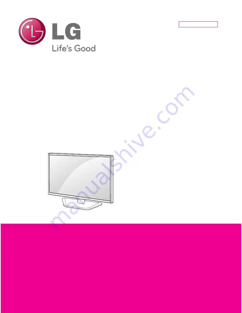
CHASSIS : LT33B
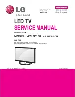
MODEL : 42LN5700
42LN5700-DH
CAUTION
BEFORE SERVICING THE CHASSIS,
READ THE SAFETY PRECAUTIONS IN THIS MANUAL.
LED TV
SERVICE MANUAL
North/Latin America
http://aic.lgservice.com
Europe/Africa
http://eic.lgservice.com
Asia/Oceania
http://biz.lgservice.com
Internal Use Only
Summary of Contents for 42LN5700
Page 60: ......


