background image

89

Plasma Fall 2008 42PG20

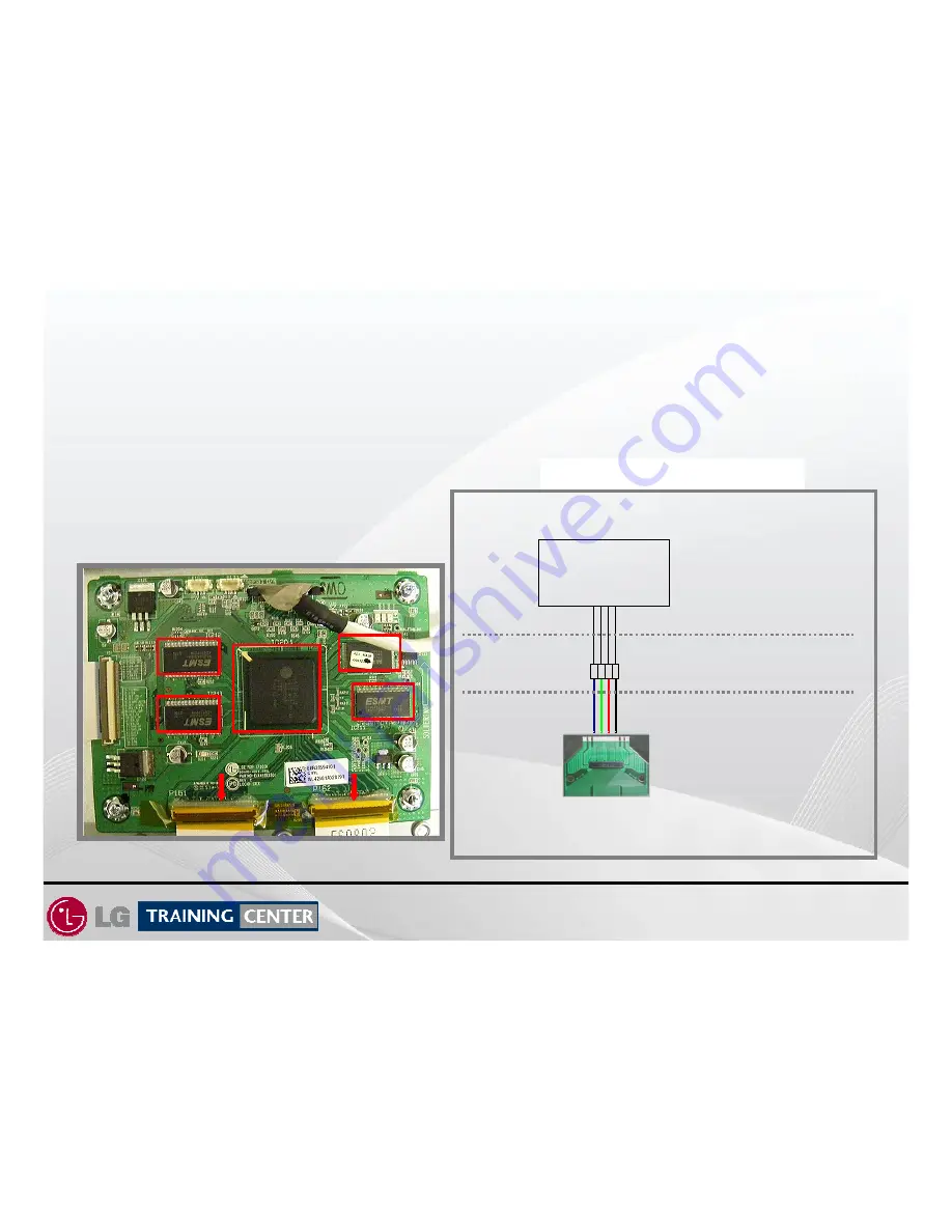
This Picture shows Signal Flow Distribution to help determine the 

failure depending on where the it shows on the screen.

The Control Board supplies Video Signals to the TCP (Tape Carrier Package) ICs. 

If there is a bar defect on the screen, it could be a Control Board problem.

MCM

16 line

Resistor Array

192 Lines output Total

Diagram of Control Board 

Control Board to X Board 

Address Signal Flow

IC201

Control PWB Signal Block

Control PWB Signal Block

MCM

DRAM

DRAM

DRAM

EEPROM

2 Buffer 
Outputs 
per TCP

CONTROL PWB

X-DRIVE PWB

PANEL

96 Lines per Buffer

Summary of Contents for 42PG20 Series

Page 1: ...1 Advanced Single Scan Troubleshooting Training Manual 42PG20 Plasma Display 42PG20 Plasma Display 720p 720p ...

Page 2: ...rive signals from Y SUS PWB Control Board Outputs Y and Z control signals to Y SUS PWB X Drive Boards 2 Circuit Board Operation Troubleshooting and Alignment of Switch mode Power Supply Main Board Section 1 Section 2 Contact Information Preliminary Matters Specifications Plasma Overview General Troubleshooting Steps Disassembly Instructions Voltage and Signal Distribution OUTLINE OUTLINE NEW NEW N...

Page 3: ...n save time and money sometimes can be overlooked These techniques will also be presented This Section will get the Technician familiar with the Disassembly Identification and Layout of the Plasma Display Panel At the end of this Section the Technician should be able to Identify the Circuit Boards and have the ability and knowledge necessary to safely remove and replace any Circuit Board or Assemb...

Page 4: ...lectronics Unauthorized modifications will not only void the warranty but may lead to property damage or user injury If wires screws clips straps nuts or washers used to complete a ground path are removed for service they must be returned to their original positions and properly fastened CAUTION CAUTION To avoid personal injury disconnect the power before servicing this product If electrical power...

Page 5: ...ce pursuant to Part 15 of the FCC Rules These limits are designed to provide reasonable protection against harmful interference when the equipment is operated in a residential installation This equipment generates uses and can radiate radio frequency energy and if not installed and used in accordance with the instruction manual may cause harmful interference to radio communications However there i...

Page 6: ...00 Technical Support and Part Sales 800 847 7597 USA Website GCSC aic lgservice com Customer Service Website us lgservice com LG CS Academy lgcsacademy com LG Web Training lge webex com Published March 2009 by LG Technical Support and Training LG Electronics Alabama Inc 201 James Record Road Huntsville AL 35813 ...

Page 7: ...ts are completely discharged because of residual current stored before Circuit Board removal 4 C MOS circuits are used extensively for processing the Drive Signals and should be protected from static electricity 5 The PDP Module must be carried by two people Always carry vertical NOT horizontal 6 The Plasma television should be transported vertical NOT horizontal 7 Exercise care when making voltag...

Page 8: ...examination using your senses the first check should always be the DC Supply Voltages to those circuits under test Always confirm the supplies are not only the proper level but be sure they are noise free If the supplies are missing check the resistance for possible short circuits Isolate To further isolate the failure check for the proper waveforms with the Oscilloscope to make a final determinat...

Page 9: ...9 Plasma Fall 2008 42PG20 This section of the manual will discuss the specifications of the 42PG20 Advanced Single Scan Plasma Display Panel 42PG20 Product Information 42PG20 Product Information ...

Page 10: ...p HD Resolution Dual XD Engine 20 000 1 Contrast Ratio Fluid Motion 3x HDMI V 1 3 with Deep Color AV Mode Cinema Sports Game Clear Voice LG SimpLink Connectivity Invisible Speaker System 100 000 Hours to Half Brightness Typical PC Input 720P PLASMA HDTV 42 Class 41 5 diagonal ...

Page 11: ...a wide screen high resolution video image coupled with multi channel compact disc quality sound FORMATS 480I 480P 1080I 720P 1080P Interlaced Progressive Interlaced Progressive Progressive Interlaced 2 Fields to make a Frame Progressive Each Field is a Frame Think of sync as the Panels Refresh Rate 240 Lines 480 Lines 540 Lines 720 Lines 1080 Lines NTSC SD HD HD HD BASIC PIXEL COUNTS PLASMA 1365 H...

Page 12: ... multi connectivity HDMI 1 3 Deep color provides a wider bandwidth 340MHz 10 2Gbps than that of HDMI 1 2 delivering a broader range of colors and also drastically improves the data transmission speed Dual XD Engine Realizing optimal quality for all images One XD Engine optimizes the images from RF signals as another XD Engine optimizes them from External inputs Dual XD Engine presents images with ...

Page 13: ...r dialogue sound Automatically enhances and amplifies the sound of the human voice frequency range to provide high quality dialogue when background noise swells Save Energy Save Money Home electronic products use energy when they re off to power features like clock displays and remote controls Those that have earned the ENERGY STAR use as much as 60 less energy to perform these functions while pro...

Page 14: ... Dolby Digital In thousands of cinemas and millions of homes worldwide Dolby Digital is the reigning standard for surround sound technology in general and 5 1 channel surround sound in particular FluidMotion 180 Hz Effect Invisible Speaker Personally tuned by Mr Mark Levinson for LG TAKE IT TO THE EDGE newly introduces Invisible Speaker system guaranteeing first class audio quality personally tune...

Page 15: ... is 5 44 milliseconds Panel Response Time is less than 1 millisecond FluidMotion 180 Hz Effect Enjoy smoother clearer motion with all types of programming such as sports and action movies The moving picture resolution give the impression of performance of up to 3x the panels actual refresh rate 42PG20 Specifications 42PG20 Specifications FluidMotion FluidMotion Familiarization Familiarization ...

Page 16: ...16 Plasma Fall 2008 42PG20 42PG20 Remote Control 42PG20 Remote Control TOP PORTION BOTTOM PORTION ...

Page 17: ...17 Plasma Fall 2008 42PG20 Rear Input Jacks Rear Input Jacks ...

Page 18: ...18 Plasma Fall 2008 42PG20 42PG20 Dimensions 42PG20 Dimensions ...

Page 19: ...oard Identification of the 42PG20 Advanced Single Scan Plasma Display Panel Upon completion of this section the Technician will have a better understanding of the disassembly procedures the layout of the printed circuit boards and be able to identify each board DISASSEMBLY SECTION DISASSEMBLY SECTION ...

Page 20: ...G20 Removing the Back Cover To remove the back cover remove the 26 screws The Stand does not need to be removed Indicated by the arrows PAY CLOSE ATTENTION TO THE TYPE SIZE AND LENGTH Of the screws when replacing the back cover Improper type can damage the front ...

Page 21: ...rcuit Board Layout Y SUS Z SUS Drive Z SUS Right X Left X Main Digital FPC Control Logic Power Supply FPC FPC FPC FPC FPC Panel ID Label Panel Voltage Label Side Input part of main Y Drive Control Keys Power Button Invisible Speakers TCP Heat Sink Z drive from Y SUS ...

Page 22: ...are CMOS and prone to static failure Disassembly Procedure for Circuit Board Removal Disassembly Procedure for Circuit Board Removal Disconnect the following connectors P201 P801 P101 P202 Remove the 8 screws holding the PWB in place Remove the PWB When replacing be sure to readjust the Va Vs voltages in accordance with the Panel Label Confirm VSC Vy and Zbias as well Disconnect the following Flex...

Page 23: ...K501 Remove the 2 screws holding on the decorative plastic piece on the right side Remove the 4 screws holding the PWB in place and Remove the PWB Disconnect the following connectors P121 P160 P161 and P162 Remove the 4 screws holding the PWB in place Remove the PWB X Drive Boards Removal Disconnect the following connectors P232 P211 P311 and P331 Remove the 13 screws holding the Heat Sink in plac...

Page 24: ...t jacks Marked B and remove D Remove the 2 screws at the top of the Main Board Mounting Bracket and peel the tape from the bottom Remove connector P303 and JK501 Carefully reposition the Main Board and Mounting Bracket up and off to the right side E Remove the metal support Brackets marked E F Remove the 13 screws holding the Heat Sink and carefully lift it straight up and off remember that the TC...

Page 25: ... the Brackets and Assemblies marked with A F will need to be removed this includes the Stand Before an X Board can be removed the Heat Sink Assembly F must be removed X Circuit Board Removal X Circuit Board Removal Y and Z SUS Drive Z SUS E Right X Left X Main Digital Control Logic Power Supply Y Drive E B F D C A ...

Page 26: ...the locking mechanism upward Gently lift the locking mechanism upward on all TCP connectors P201 206 or P301 306 Carefully lift the TCP ribbon up and off the cushion and out of the way TCP Flexible ribbon cable After removing the back cover Main PWB is lifted out of the way 15 screws removed from heat sink covering TCPs and heat sink removed the X Drive PWBs can be removed Cushion ...

Page 27: ...er Carrier Package Precautions Package Precautions TCP Connector Removal Lift up the lock as shown by arrows The Lock can be easily broken It needs to be handled carefully Pull TCP apart as shown by arrow TCP Film can be easily damaged Handle with care ...

Page 28: ...ight X Drive Removal Left and Right X Drive Removal Remove the 5 screws for either PWB or 9 total for both The Center screw secures both PWBs Right X Board drive the left side of the screen Left X Board drives the right side of the screen ...

Page 29: ...29 Plasma Fall 2008 42PG20 Signal and Voltage Distribution Signal and Voltage Distribution SLIDE CORRECTED HANDOUT MANUAL ERROR ...

Page 30: ...nderstand the operation of each circuit board and how to adjust the controls The technician should be able with confidence to troubleshoot a circuit board failure replace the defective circuit and perform all necessary adjustments SECTION 2 CIRCUIT OPERATION TROUBLESHOOTING AND SECTION 2 CIRCUIT OPERATION TROUBLESHOOTING AND CIRCUIT ALIGNMENT SECTION CIRCUIT ALIGNMENT SECTION Remember the Z SUS Dr...

Page 31: ...DC Va Vs 5 Adjusting Voltage Set Up Vy Vsc Ve Vzb 6 Trade name of LG Electronics 7 Manufactured date Year Month 8 Warning PANEL LABEL EXPLANATION PANEL LABEL EXPLANATION 9 TUV Approval Mark 10 UL Approval Mark 11 UL Approval No 12 Model Name 13 Max Watt Full White 14 Max Volts 15 Max Amps ...

Page 32: ...s encountered 4 As a general rule of thumb when ever the back is removed Remember the Voltage Label MUST be followed it is specific to the panel s needs All label references are from a specific panel They are not the same for every panel encountered VY Z_BIAS Panel Rear View Manufacturer Bar Code Set Up Ve Vscan The Waveform adjustment is only necessary 1 When the Y SUS PWB is replaced 2 When a Ma...

Page 33: ...r Label location identification and are not used with this panel VY Vscan Z_BIAS 42PG20 SWITCH MODE POWER SUPPLY Troubleshooting SWITCH MODE POWER SUPPLY Troubleshooting This Section of the Presentation will cover troubleshooting the Switch Mode Power Supply for the Single Scan Plasma Upon completion of the section the technician will have a better understanding of the operation of the Power Suppl...

Page 34: ...k the sticker on the upper left side to confirm origin of the Panel or the White Label on the Power Supply itself to identify the PWB P N We will examine the Operation of the EAY43533901 Switch Mode Power Supply Part Number Switch Mode Power Supply Part Number ...

Page 35: ...Gnd Gnd 5_V Det RL_ON M5V_ON 2 4 6 8 10 12 14 16 18 20 22 16 5V Gnd 0V Gnd 5V 5V Gnd Gnd AC Det VS_ON Gnd 1 16 5V Power Supply PWB Layout Power Supply PWB Layout 1 2 3 4 5 6 7 8 9 10 Vs Vs n c GND GND Va Va GND M5V M5V P812 P813 Hot Ground Symbol represents a SHOCK Hazard ...

Page 36: ... Used to develop Bias Voltages on the Y SUS X Drive and Control Boards 16V Audio B Supply 5V Signal Processing Circuits Adjustments There are 2 adjustments located on the Power Supply Board VA and VS The 5V VCC is pre adjusted and fixed All adjustments are made with relation to Chassis Ground Use Full White Raster 100 IRE VA VS RV901 RV951 Switch Mode Power Supply Overview Switch Mode Power Supply...

Page 37: ... CN 101 P812 380V Source AC Input VS Source VA Source Standby Source 16v 5v Source IC701 Sub Micon VA VR901 P813 10Amp 230V Switch Mode Power Supply Circuit Layout Switch Mode Power Supply Circuit Layout PFC Circuit 340V Fuse F801 10Amp 230V To Y Z SUS To MAIN ...

Page 38: ...s a high to RL ON This signal first turns on a DC level shifter Q706 which creates 5V General LD703 now glows amber indicating 5V General has been generated This 5V General now provides the pull up voltages when supply the output circuits to the SMPS The RL ON enters the SMPS Board at Pin 19 of P813 The RL ON Voltage is sensed by the Sub Micon IC701 circuit which causes the Relay Drive Circuit to ...

Page 39: ... Video Circuits on the Main Board to function and if connected to an Antenna Input Audio would be present If the Relays closed and these supplies failed suspect a problem with the SMPS The next step of operation calls for the M5V_ON line from the Main Board to the SMPS to go high on P813 pin 21 A high on the M5V_ON Line activates the 5V VCC line Loss of 5V VCC results in no Raster no Display Panel...

Page 40: ...eg Vs Reg Va Reg 12V 16V Regulators 5V Det 5V Reg Stand By 5V Reg 1 2 3 5 5 6 6 7 9 8 10 2 5 4 Both LEDs On Looks Amber NOTE 1 50PG20 has 12V and 16V to Main at turn on 42PG20 only has 16V At point TV is in Stand By state Energy Star compliant Less than 1 Watt 50PG20 42PG20 POWER SUPPLY TURN ON COMMANDS FROM MAIN PWB 5 5 9 7 In Stand By Primary side is 90V In Run Relay On Primary side is 370V 3 Tu...

Page 41: ...41 Plasma Fall 2008 42PG20 Microprocessor Side Microprocessor Side Control of the Switch Control of the Switch Mode Power Supply Mode Power Supply See next Slides Closer View ...

Page 42: ...42 Plasma Fall 2008 42PG20 Microprocessor Side Microprocessor Side Control of the SMPS Control of the SMPS Step 1 Step 1 ...

Page 43: ...43 Plasma Fall 2008 42PG20 Microprocessor Side Control of the SMPS Step 2 Microprocessor Side Control of the SMPS Step 2 ...

Page 44: ...Mode Power Supply Static Test If the Y SUS Z SUS and X PWBs are working normal when the SMPS comes up to full power on Display Panel Reset will be visible Shorting the Auto Pattern Gen test points at this time should result with test patterns on the screen If either Y SUS or Z SUS is causing the power supply to shutdown unplug the Z SUS Remember Vs is routed to the small vertical Z SUS PWB P1 pin ...

Page 45: ...45 Plasma Fall 2008 42PG20 STATIC TEST UNDER LOAD LIGHT BULB TEST ...

Page 46: ...er Supply Static Test Forcing on the SMPS in stages ges AC Power Applied AC Det Pin 18 and 5V STB Pins 9 12 are 5V 100Ω watt resistor added from 5V STB Pins 9 12 to RL ON Pin 19 closes relay RL101 turning on the 16V Supply 100Ω watt resistor added from 5V STB Pins 9 12 to VS _ON Pin 20 brings the VA and VS Lines high 100Ω watt resistor added from 5V STB Pins 9 12 to M5V_ ON Pin 21 brings the 5V VC...

Page 47: ...ply AC Power Power Supply Starts Vs TP P812 Pin 1 or 2 This Power Supply will come up and run with NO load P812 pulled Use Full White Raster Va and Vs Adjustments Va and Vs Adjustments Y Z SUS Runs Yes Both Y and Z waveforms Generated Yes Va TP P812 Pin 5 or 6 ...

Page 48: ...Measurements for the SMPS All voltages from a working unit All resistance from disconnected PWB Note This voltage will vary in accordance with Panel Label 1 37V 5V 0V M5V 10 1 47V 5V 0V M5V 9 Gnd 0V 0V Gnd 8 Open 65V 0V Va 7 Open 65V 0V Va 6 Gnd 0V 0V Gnd 5 n c n c n c n c 4 Gnd 0V 0V Gnd 3 Open 195V 0V Vs 2 Open 195V 0V Vs 1 Diode Mode Run STBY Label Pin P812 CONNECTOR Power Supply PWB to Y SUS ...

Page 49: ... P803 Odd Pins ID and Voltages Open 0V 3 24V 0V M5V_ON 21 Open 0V 3 73V 0V RL_On 19 1 92V 5V 5V 15V 5_V Det 17 Gnd Gnd Gnd Gnd Gnd 15 Gnd Gnd Gnd Gnd Gnd 13 1 43V 5V 5V 5V 5V 11 1 43V 5V 5V 5V 5V 9 Gnd Gnd Gnd Gnd Gnd 7 Open NC NC NC NC 5 Gnd Gnd Gnd Gnd Gnd 3 1 5V 16 5V 16 5V 0V 15V 1 Diode Mode No Load Run STBY Label Pin P813 CONNECTOR Odd SMPS to P701 Main PWB ...

Page 50: ...ges P803 Even Pins ID and Voltages Open 5V 0V 0V AUTO 22 Open 0V 3 2V 0V Vs_On 20 2 3V 5V 5V 5V AC Det 18 Gnd Gnd Gnd Gnd Gnd 16 Gnd Gnd Gnd Gnd Gnd 14 1 43V 5V 5V 5V 5V 12 1 43V 5V 5V 5V 5V 10 Gnd Gnd Gnd Gnd Gnd 8 Open NC NC NC NC 6 Gnd Gnd Gnd Gnd Gnd 4 1 5V 16 5V 16 5V 0V 15V 2 Diode Mode No Load Run STBY Label Pin P813 CONNECTOR Even SMPS to P701 Main PWB ...

Page 51: ...n relay opens it drops to 155V Using the Front Power LED for visual clues Using the Front Power LED for visual clues 3 16V Short Power LED is lit Red in stand by At Power On Power LED cycles Red and Blue Relay clicks rapidly on and off STBY 5V line toggles with relay from 2 2V to 5V 4 5Vcc Short Power LED is lit Red in stand by At Power On goes to flashing Blue 5Vcc line toggles rapidly between 0V...

Page 52: ...ng Voltages Voltages SMPS Supplied VA VS VCC M5V Y Z SUS Developed VY V SET UP VR602 V SET DN VR601 VSC 16V VA supplies the Panel Vertical Grid VS Supplies the Panel Horizontal Grid 5V Supplies Bias to Y Z SUS Control via the Y SUS VY Sets the Negative excursion of the Y SUS Drive Waveform Ramp UP sets Pitch of the Top Ramp of the Drive Waveform V Set Down sets the Pitch of the Bottom Ramp of the ...

Page 53: ...Ramp Up Down Control Board Circuits generate Y Sustain Waveform Distributes 5V VS Distributes 5V Logic signals needed to generate drive waveform Distributes 16V and VA Receive 5V VCC Va Vs from SMPS Transfer Waveform to Y Drive Board Z SUS Section on the Same PWB Right X Board Display Panel Power Supply Board SMPS FETs amplify Sustain Waveform Left X Board ...

Page 54: ... VSC VY To Y Drive To Y Drive V SET DN VR 601 Y Y SUS PWB Layout SUS PWB Layout P801 Logic Signals from the Control PWB P202 16V and Va to Left and Right X PWBs Logic Drive Signals to the Y Drive PWBs Use Y Drive Waveform TP VSC TP R211 VY TP R210 Z Drive to Z Output PWB P101 Z Bias ADJ VR905 FS701 Va 10A FS201 5A ZBias TP R946 ...

Page 55: ...ltage Adjustments VSC VY Lower Left Side of PWB VSC TP R211 Middle Left Side of PWB Vy TP R210 Voltage Reads Positive VR501 Vsc TP VR502 Vy TP Set should run for 15 minutes this is the Heat Run mode Set screen to White Wash mode or 100 IRE White input Adjust Vy to 190V 1V Adjust VSC to 140 1V Heat Run Vs Va adjustments should have been completed ...

Page 56: ...oint c Overall signal observed 2mS div dHighlighted signal from figure above observed 200uS div e Highlighted signal from figure above observed 100uS div NOTE If Vset DN too high this set will go to excessive bright then shutdown To correct remove the LVDS from control PWB and make necessary adjustments ...

Page 57: ...2ms per div the signal for Vsetup is now easier to recognize It is outlined within the Waveform Fig 3 Top At 1ms per div the signal for Vsetup is now clearly visible It is outlined within the Waveform Fig 3 Lower At 40uSec per division the adjustment for Vsetup can be made Fig 2 Lower At 100uSec per division the waveform to use for Vsetup Is now isolated Fig 1 Lower At 400uSec per division the wav...

Page 58: ...r div the outlined signal for Vsetdn is now easier to recognize It is outlined within the Waveform Fig 1 Top At 1ms per div the outlined signal for Vsetdn is now clearly visible It is outlined within the Waveform Fig 1 Lower At 40uSec per division the adjustment for Vsetdn can be made Fig 1 Lower At 100uSec per division the waveform to use for Vsetdn Is now isolated Fig 1 Lower At 400uSec per divi...

Page 59: ...S Vs Va VSC VSC Vy and Z Bias Must have already been completed Observe the Picture while making these adjustments Normally they do not have to be done V V Set Up RAMP and V Set Up RAMP and V Set Down Adjustments Set Down Adjustments Y Drive PWB Test Point ...

Page 60: ...idens due to the Vset UP peeking too quickly The center begins to wash out and arc due to Vset UP Peeking too late and alters the start of the Vset DN phase Panel Waveform Adjustment Ramp Vset UP too high Ramp Vset UP too low V Set Up Too High or Low V Set Up Too High or Low Vset UP swing is Minimum 150vP P Max 220vP P ...

Page 61: ...e to decreased Vset DN time Panel Waveform Adjustment Vset DN too low Vset DN too high V Set V Set Dn Dn Too High or Low Too High or Low Vset Dn swing is Minimum 60uS Max 123uS NOTE If Vset DN too high this set will go to excessive bright then shutdown To correct remove the LVDS from control PWB and make necessary adjustments ...

Page 62: ...igh Approx 120uSec This is the Shutdown Threshold level Any higher the set will shut down Notice that the amplitude of the Set Down Bottom portion peak begins to decrease Time Time Peak GOOD NO GOOD NOTE If Vset DN too high this set will go to excessive bright then shutdown To correct remove the LVDS from Control PWB and make necessary adjustments 50V per Division 5V per Division 50V per Division ...

Page 63: ... P812 Plug Information SUS P201 to SMPS P812 Plug Information Note This voltage will vary in accordance with Panel Label 83V 5V 0V M5V 10 83V 5V 0V M5V 9 Gnd 0V 0V Gnd 8 Open 65V 0V Va 7 Open 65V 0V Va 6 Gnd 0V 0V Gnd 5 Gnd 0V 0V Gnd 4 NC NC NC NC 3 Open 194V 0V Vs 2 Open 194V 0V Vs 1 Diode Mode Run STBY Label Pin P201 CONNECTOR Y SUS to Power Supply PWB P812 ...

Page 64: ... and P311 Plug Information Note This voltage will vary in accordance with Panel Label Open 64 9V 0V Va 12 Open 61 5V 0V ER1 11 Open 61 5V 0V ER1 10 1V 15 8V 0V 15V 9 Gnd Gnd Gnd Gnd 8 Gnd Gnd Gnd Gnd 7 Open 64 9V 0V Va 6 Open 61 5V 0V ER2 5 Open 61 5V 0V ER2 4 1V 15 8V 0V 15V 3 Gnd Gnd Gnd Gnd 2 Gnd Gnd Gnd Gnd 1 Diode Mode Run STBY Label Pin P202 CONNECTOR Y SUS PWB to X Drive Left P211 and Right...

Page 65: ...on SUS P801 to Z Drive P1 Plug Information Note This voltage will vary in accordance with Panel Label Open 70 46V 0V ZSUS 11 Gnd Gnd Gnd Gnd 10 Open 70 46V 0V ZSUS 9 Gnd Gnd Gnd Gnd 8 Open 70 46V 0V ZSUS 7 Gnd Gnd Gnd Gnd 6 Open 70 46V 0V ZSUS 5 Gnd Gnd Gnd Gnd 4 Open 70 46V 0V ZSUS 3 Gnd Gnd Gnd Gnd 2 Open 194V 0V Vs 1 Diode Mode Run STBY Label Pin P801 Connector Y SUS to Z Drive P1 Plug Informat...

Page 66: ... P160 Plug Information SUS to Control PWB P160 Plug Information These connector pins are too close to read without possible damage to the PWB Actually a 60 Pin Connector Only Labels for 1 19 on the Control PWB Looking closely these test points are every other pin The bottom TP represents 19 label on the Control PWB ...

Page 67: ... 9V 0V X_ER 36 Gnd Gnd Gnd Gnd 35 2 87V 1 4V 0V Set_DN_2 34 Gnd Gnd Gnd Gnd 33 2 87V 1 9V 0V SET_UP 32 Gnd Gnd Gnd Gnd 31 2 87V 0V 0V SLOPE_RETE 30 Gnd Gnd Gnd Gnd 29 2 87V 0V 0V DET_LEVEL 28 Gnd Gnd Gnd Gnd 27 2 87V 0 16V 0V DELTA_Vy 26 Gnd Gnd Gnd Gnd 25 2 87V 0 2V 0V PASS_TOP 24 Gnd Gnd Gnd Gnd 23 2 87V 0 2V 0V Set_DN2 22 Gnd Gnd Gnd Gnd 21 Diode Mode Run STBY Label Pin Gnd Gnd Gnd Gnd 60 1 1V ...

Page 68: ...to Check the Output FETs Name is printed on the components 30F122 Forward 0 5V 0 7V Reverse OL 30F122 Forward 0 4V 0 5V Reverse OL RF2001 Forward 0 3V 0 5V Reverse OL RF2001 Forward 0 3V 0 5V Reverse OL 45F123 Forward 0 3V 0 5V Reverse OL 45F123 Forward 0 9V 1 0V Reverse OL ...

Page 69: ...AIN PWB and sent to the Panel through SCAN DRIVER IC s The Y Drive Boards supply a waveform which selects the horizontal electrodes sequentially 42PG20 uses 8 DRIVER ICs on 1 Y Drive Board Y Drive Board Explained Y Drive Board Explained Y DRIVE WAVEFORM To facilitate scope attachment solder a small wire Stand Off at this point ...

Page 70: ...Connectors P200 Logic Signals from P100 Y Drive PWB ID Y Drive PWB ID P200 Y Drive and Logic Signals Clock and Data from the Y SUS Board TOP BOTTOM Check 5V supply using FL1 or C18 Measured from Floating Ground Floating Ground from the Y SUS Board PANEL SIDE Y SUS SIDE Floating Ground from the Y SUS Board Y Drive Sig Scan ...

Page 71: ...Back and Front of Connector Identical Connector Identical All voltages taken All voltages taken from Floating from Floating Ground Ground Warning Do not Warning Do not hook scope ground hook scope ground up unless set up unless set plugged into an plugged into an isolation isolation transformer transformer ...

Page 72: ...einstall the Ribbon Cable carefully slide it back into the slot see Fig 3 be sure the Tab is seated securely and press the Locking Tab back to the locked position see Fig 2 then Fig 1 Removing Panel Flexible Ribbon from Y Drive Removing Panel Flexible Ribbon from Y Drive Flexible Ribbon Cables shown are from a different model but pro Flexible Ribbon Cables shown are from a different model but proc...

Page 73: ...er a greater resistance to closing in the case Note the cable is crooked In this case the Tab on the Ribbon cable was improperly seated at the bottom This can cause bars lines intermittent lines abnormalities in the picture Remove the ribbon cable and re seat it correctly Y Drive Flexible Ribbon Incorrectly Seated Y Drive Flexible Ribbon Incorrectly Seated ...

Page 74: ...K LEAD ON A FORWARD READING 0 73V REVERSE READING OPEN OL BACK or FRONT SIDE OF Y DRIVE PWB Any where A B VSC n c FLOATING GND n c Osc2 In Osc1 In LE In CLK In DATA In n c n c 5V BLACK LEAD ON B RED LEAD ON A Additional Readings RED LEAD ON B 0 57V Black on Osc2 0 59V Black on Osc1 0 58V Black on LE 0 60V Black on CLK 0 78V Black on DATA 0 50V Black on 5V BLACK LEAD ON B OL Red on Osc2 OL Red on O...

Page 75: ...D ON ANY OUTPUT LUG READING 0 73 V OUTPUT LUGS BLACK LEAD ON BUFFER IC RED LEAD ON ANY OUTPUT LUG READING OPEN YOU CAN CHECK ALL 8 BUFFER ICs USING THIS PROCEDURE YOU CAN CHECK ALL 8 BUFFER ICs USING THIS PROCEDURE Any of these output lugs can be tested Look for shorts indicating a defective Buffer IC Indicated by white outline BACK SIDE OF Y DRIVE PWB Indicated by white outline Floating Ground ...

Page 76: ...the Y Z Z SUS Board SUS Board Assembly Upon completion of this section the Technician will ha Assembly Upon completion of this section the Technician will have a better understanding of the ve a better understanding of the circuit and be able to locate voltage and resistance test points circuit and be able to locate voltage and resistance test points needed for troubleshooting and needed for troub...

Page 77: ... PWB P801 Logic Signals from the Control PWB P202 16V and Va to Left and Right X PWBs VZ Z Bias Z Drive to Z SUS Output PWB P101 FS701 Va 10A FS201 5V 5A VZ Z Bias TP R946 ZBias TP R946 Read the Label on the back of the upper left hand side of the panel Adjust R946 to that voltage Z SUS Section Y SUS Section Y SUS Output ICs Z Bias ADJ VR905 No IPMs ...

Page 78: ...d Circuit Scope Probe connect point bottom leg of R1 to check Z Output waveform Z Z SUS Waveform SUS Waveform Z Bias is a DC adjustment The effects of this adjustment can be observed on the scope looking at the Z SUS output Z SUS PWB This Waveform is just for reference to observe the effects of Zbz adjustment Vzb voltage 1V 100V Z Drive Waveform Vzb Z Bias VR905 2 mS div Note The Vzb Adjustment is...

Page 79: ...ment P801 To Z SUS VZ Z Bias VZ Z Bias TP R946 Read the Label on the back of the upper left hand side of the panel Adjust R946 to that voltage Set should run for 15 minutes this is the Heat Run mode Set screen to White Wash mode or 100 IRE White input Adjust VZ Z Bias to 100V 1V ...

Page 80: ...ng SUS PWB Understanding The Z The Z SUS Board in this model is only a small vertical board with outp SUS Board in this model is only a small vertical board with output FETs ut FETs Drive waveforms are generated on the Y Drive waveforms are generated on the Y SUS PWB SUS PWB Z Drive Signals to Power FET s Input Signals from the Y SUS Board Input Signals from the Y SUS Board ...

Page 81: ... Diagram SUS Board Block Diagram Circuits generate erase sustain waveforms Generates Z Bias 100V Distributes Logic Signals M5V VA VS FET Makes Drive waveform Display Panel Via FPC flexible printed circuit Control Board Y SUS Board Z SUS FETs Via P801 to P1 NO IPMs Z SUS PWB Z SUS Section of the Y SUS PWB Receives VS VA M5V ...

Page 82: ...e Voltage and Resistance Measurements Note This voltage will vary in accordance with Panel Label Open 70 46V 0V ZSUS 11 Gnd Gnd Gnd Gnd 10 Open 70 46V 0V ZSUS 9 Gnd Gnd Gnd Gnd 8 Open 70 46V 0V ZSUS 7 Gnd Gnd Gnd Gnd 6 Open 70 46V 0V ZSUS 5 Gnd Gnd Gnd Gnd 4 Open 70 46V 0V ZSUS 3 Gnd Gnd Gnd Gnd 2 Open 194V 0V Vs 1 Diode Mode Run STBY Label Pin P801 CONNECTOR Y SUS PWB to Z SUS Out P1 ...

Page 83: ...ped on the 1 8V Control board 2 3 3V This Section of the Presentation will cover troubleshooting the Control Board Assembly Upon completion of this section the Technician will have a better understanding of the circuit and be able to locate voltage and resistance test points needed for troubleshooting Main Board Supplied LVDS Signal Operating Voltages Operating Voltages ...

Page 84: ...ft To X Drive Right P164 P131 IC201 MCM P121 IC212 IC213 IC121 IC101 IC211 IC171 IC122 IC133 AUTO GEN TEST PATTERN Control PWB Identified Control PWB Identified Download Connection To P101 Y SUS 5V Part Number Label 3 3V 0V n c 5V 3 3V 0V IC171 Pin 1 3 29V Pin2 1 20v Pin 3 0V 3 3V VS_DA 3V 3 3V ...

Page 85: ...85 Plasma Fall 2008 42PG20 Control PWB Pictorial Control PWB Pictorial IC121 Pin 1 4 75V Pin 2 3 3V Pin 3 0V Note P812 on SMPS P201 on Y SUS IC122 Pin 1 4 75V Pin 2 3 3V Pin 3 0V ...

Page 86: ...on has a problem related to 1 Shutdown caused by Main PWB 2 No Picture This can be checked by the following 1 Disconnect the Main PWB from all connectors Apply AC power Since P813 is not connected the set will come on Short the two pins on the Auto Test Pattern lands If there is a picture of cycling colors the Y SUS Y Drive Z SUS Power Supply Control PWBs and Panel are all OK Same test for 2 to te...

Page 87: ...k the output of the Oscillator package The frequency of the sine wave is 50 MHZ Missing this clock signal can halt operation of the unit Osc Check 50Mhz Checking the Crystal Checking the Crystal Clock Clock DC Voltage Check 1 5V 1 8V ...

Page 88: ...hile pressing the Menu Button on and off with the Remote Control or Keypad Loss of these Signals would confirm the failure is on the Main Board Example of Normal Signals measured at 200mv cm at 5µs cm Menu Off Menu ON LVDS Cable P121 on Control PWB shown Press two outside tabs inward to release Control LVDS Signals Control LVDS Signals 1 3 5 7 9 11 13 15 17 19 21 2 4 6 8 10 12 14 16 18 20 22 Conne...

Page 89: ... to the TCP Tape Carrier Package ICs If there is a bar defect on the screen it could be a Control Board problem MCM 16 line Resistor Array 192 Lines output Total Diagram of Control Board Control Board to X Board Address Signal Flow IC201 Control PWB Signal Block Control PWB Signal Block MCM DRAM DRAM DRAM EEPROM 2 Buffer Outputs per TCP CONTROL PWB X DRIVE PWB PANEL 96 Lines per Buffer ...

Page 90: ...two Interlocks that must be disengaged to remove the LVDS Cable To Disengage press the two Locking Tabs Inward and pull the plug out Removing the LVDS Cable from the Control PWB Removing the LVDS Cable from the Control PWB Press Inward Press Inward ...

Page 91: ...V 23 1V 0V 0V 21 Gnd Gnd Gnd 19 1V 0V 0V 17 1V 0V 0V 15 Gnd Gnd Gnd 13 1V 1 15V 0V 11 1V 0V 0V 9 1V 1 26V 0V 7 1V 1 19V 0V 5 1V 0V 0V 3 Gnd Gnd Gnd 1 Diode Mode Run SBY Pin P121 CONNECTOR Odd Pins Control to P302 Main Open 0V 0V 30 Open 3 29V 0 89V 28 Gnd Gnd Gnd 26 1V 1 26V 0V 24 2 5V 0 56V 0 89V 22 1V 0 21V 0V 20 1V 0V 0V 18 1V 0V 0V 16 Gnd 0V 0V 14 1V 1 26V 0V 12 1V 0V 0V 10 1V 1 19V 0V 8 Gnd 0...

Page 92: ... 4 Z SUS UP 5 ground etc Remember this connector has many more pins than the labels indicate This shows the Pin Labeling that is shown on the silk screening This connector is a little confusing in its labeling It is actually a 60 pin connector This labeling refers to P160 pin ID This too has ground between each pin These are responsible for Z Drive signals 14 Pins related to Z SUS 39 Pins related ...

Page 93: ...30 1 34V 1 9V 0V SET_UP 29 Gnd Gnd Gnd Gnd 28 1 34V 1 4V 0V Set_DN_2 27 Gnd Gnd Gnd Gnd 26 1 33V 2 9V 0V X_ER 25 Gnd Gnd Gnd Gnd 24 1 33V 0 6V 0V Y Enable 23 n c n c n c n c 22 1 06V 4 75V OV 5V 21 Diode Mode Run STBY Label Pin Gnd Gnd Gnd Gnd 60 1 34V 3 2V 0V CLK 59 Gnd Gnd Gnd Gnd 58 1 34V 0 76V 0V STB 57 Gnd Gnd Gnd Gnd 56 1 34V 0V 0V OSC1 55 Gnd Gnd Gnd Gnd 54 1 34V 3V 0V OSC2 53 Gnd Gnd Gnd G...

Page 94: ...made P161 CONNECTOR Control PWB to X Drive Left P232 These pins are covered in silicon P162 CONNECTOR Control PWB to X Drive Right P331 These pins are covered in silicon Control PWB Connector P161 and P162 to X Control PWB Connector P161 and P162 to X Drive PWBs Drive PWBs ...

Page 95: ...o X Drive PWB Control PWB Connectors to X Drive PWB Power Cables Va 15V Signal cable Between Ctrl B D and X Between Ctrl B D and X B D measurements can B D measurements can t be made t be made P161 P161 P162 P162 P331 P331 P232 P232 P211 P211 P311 P311 ...

Page 96: ...US board 15V received from the Y SUS board Drive signals Color Received from the Control Board for the Vertical Grids to the TCPs DEVELOPED Developed on the X Drive boards VPP to help with over all current draw during No Video times when the panel is being driven VPP shuts off the TCPs during this time VPP is generated using Va and a drive signal from the Control board ...

Page 97: ...A Left and Right X Drive A BUS BUS TCP IC s shown are part of the Ribbon Cable TCP IC TCP IC Warning DO NOT attempt to run the set with the Heat Sink over the TCPs removed After a very short time these ICs will begin to self destruct due to overheating ...

Page 98: ...98 Plasma Fall 2008 42PG20 TCP Tape TCP Tape Carrier Carrier Package Package ...

Page 99: ...onnecting the PAD Electrode of the PANEL with the X Board TCP Connector Frame X_B D Front panel Horizontal Address Rear panel Vertical Address TCP Tape TCP Tape Carrier Carrier Package Package Control PWB Back side of Ribbon Connector into X Drive To Panel Y SUS PWB Va and 16V ...

Page 100: ...Typical Reading 0 65V Opposite reads open 5 10 15 20 25 30 35 40 45 50 1 On any Gnd On any Va 4 5 6 7 44 45 46 47 10 11 12 13 14 27 28 2 9 30 37 38 39 40 41 Look for any TCPs being discolored Ribbon Damage Cracks folds Pinches scratches etc Va Va Gnd Gnd ...

Page 101: ... shutdown b Generate abnormal vertical bars c Cause the entire area driven by the TCP to be All White d Cause the entire area driven by the TCP to be All Black e Cause a Single Line defect Warning DO NOT attempt to run the set with the Heat Sink over the TCPs removed After a very short time these ICs will begin to self destruct due to overheating ...

Page 102: ...Voltages and Resistance X Drive Left Connector P211 Voltages and Resistance Note This voltage will vary in accordance with Panel Label Open 64 9V 0V VA 8 Open 61 4V 0V VPP ER1 7 Open 61 4V 0V VPP ER1 6 n a n a 0V n c 5 n a n a 0V n c 4 Open 15 4V 0V 15V 3 Gnd Gnd 0V Gnd 2 Gnd Gnd 0V Gnd 1 Diode Mode Run STBY Label Pin P211 CONNECTOR X Drive Left to Y SUS P202 ...

Page 103: ...Voltages and Resistance X Drive Right Connector P311 Voltages and Resistance Note This voltage will vary in accordance with Panel Label Open 64 9V 0V VA 8 Open 61 4V 0V VPP ER2 7 Open 61 4V 0V VPP ER2 6 n a n a 0V n c 5 n a n a 0V n c 4 Open 15V 0V 15V 3 Gnd Gnd Gnd Gnd 2 Gnd Gnd Gnd Gnd 1 Diode Mode Run STBY Label Pin P311 CONNECTOR X Drive Right to Y SUS P202 ...

Page 104: ... P232 and P331 X Drive Left and Right Connector P232 and P331 Voltage and Resistance Measurements for these connectors are difficult to read They are too close together for safe test The pins are also protected by a layer of tape to prevent the tab from being released causing separation from the Cable and the connector ...

Page 105: ...tion of this Section the technician will have a better understanding of the operation of the circuit and will be able to locate voltage and resistance test points needed for troubleshooting and alignments 5V 3 3V 2 2 5V 1 8V 5V 12V 16V Developed on the Main Board DC Voltage and Waveform Checks Resistance Measurements Main PWB Troubleshooting Main PWB Troubleshooting ...

Page 106: ...01 P302 P303 AV In 3 To Power Supply HDMI inputs RS232 SPK Out To Front Controls JK501 Main PWB Layout and Identification Main PWB Layout and Identification X400 25 Mhz X100 12 Mhz Audio Audio RGB DVI Reset SW100 IC702 Optical Audio n USB HDMI 3 Remote A V Composite inputs LD400 LD703 Pin 1 Pin 16 ...

Page 107: ...n n IC708 n n while the PWB is turned over Location IC501 n Bottom Leg Pin 1 IC805 n Be sure to prevent the PWB from touching the frame Use a piece of cardboard or towel to insulate IC705 1 5V 2 3 29V 3 0V IC501 1 3 3V 2 1 8V 3 0V IC706 1 5V 2 2 6V 3 1 37V IC805 1 5V 2 3 3V 3 0V IC708 1 5V 2 3 31V 3 0V IC101 1 5V 2 0V 3 5V IC709 1 3 29V 2 1 26V 3 0V ...

Page 108: ...r Check Shield Off Pins Exposed Main PWB Tuner Check Shield Off Pins Exposed LD400 Tuner Osc Lock On Unlocked Off Locked X400 Tuner Controller Osc IC400 Tuner Controller VIF Pin 16 Video Test Point SIF Pin 14 Audio Test Point Pin 3 Tuner B 5V ...

Page 109: ... 42PG20 MAIN PWB Main PWB Tuner Video and SIF Output Check Main PWB Tuner Video and SIF Output Check Tuner Location 1Vp p 20uSec rate Pin 16 Video Signal Pin 14 SIF Signal 850mVp p 20nSec rate USING COLOR BAR SIGNAL INPUT ...

Page 110: ... 22V 0V 17 1 17V 1 27V 0V 15 1 17V 1 25V 0V 13 1 17V 1 25V 0V 11 1 97V 3 29V 0 89V 9 Gnd Gnd Gnd 7 Gnd Gnd Gnd 5 Open 0V 0V 3 Open 0V 0V 1 Diode Mode Run SBY Pin P302 CONNECTOR Main Odd Pins to P121 Control PWB Gnd Gnd Gnd 26 1 5V 3 29V 0 93V 24 1 17V 1 18V 0V 22 1 17V 1 21V 0V 20 1 17V 1 25V 0V 18 1 17V 1 21V 0V 16 1 17V 1 21V 0V 14 1 17V 1 21V 0V 12 1 97V 3 29V 0 89V 10 Gnd Gnd Gnd 8 Gnd Gnd Gnd...

Page 111: ...ected DVM in the Diode mode Main PWB Plug P303 Voltages Main PWB Plug P303 Voltages Gnd Gnd Gnd 12 1 03V 3 84V 0V 11 Gnd Gnd Gnd 10 1 12V 0V 0V 9 Gnd Gnd Gnd 8 0 75V 5V 5V 7 Gnd Gnd Gnd 6 1 18V 3 29V 0V 5 Gnd Gnd Gnd 4 1 18V 3 29V 0V 3 Gnd Gnd Gnd 2 2 99V 5V 5V 1 Diode Mode Run STBY Pin P303 CONNECTOR MAIN PWB to Front Keys ...

Page 112: ...s Resistance Readings with the PWB Disconnected DVM in the Diode mode 1 22V 3 24V 0V M5V_ON 21 Open 3 73V 0V RL_On 19 3 25V 5V 15V 5_V Det 17 Gnd Gnd Gnd Gnd 15 Gnd Gnd Gnd Gnd 13 0 75V 5V 5V 5V 11 0 75V 5V 5V 5V 9 Gnd Gnd Gnd Gnd 7 Open NC NC NC 5 Gnd Gnd Gnd Gnd 3 3 8V 16 5V 0V 15V 1 Diode Mode Run STBY Label Pin P701 CONNECTOR Main Odd Pins to SMPS PWB P813 ...

Page 113: ...Pins Resistance Readings with the PWB Disconnected DVM in the Diode mode Gnd Gnd Gnd AUTO 22 1 22V 3 2V 0V Vs_On 20 Open 5V 5V AC Det 18 Gnd Gnd Gnd Gnd 16 Gnd Gnd Gnd Gnd 14 0 75V 5V 5V 5V 12 0 75V 5V 5V 5V 10 Gnd Gnd Gnd Gnd 8 Open NC NC NC 6 Gnd Gnd Gnd Gnd 4 2 82V 16 5V 0V 15V 2 Diode Mode Run STBY Label Pin P701 CONNECTOR Main Even Pins to SMPS PWB P813 ...

Page 114: ...lug Main PWB Speaker Plug JK501 Voltages and Resistance Main PWB Speaker Plug JK501 Voltages and Resistance JK501 Resistance Readings with the PWB Disconnected DVM in the Diode mode 2 58V 8V 0V 4 2 58V 8V 0V 3 2 58V 8V 0V 2 2 58V 8V 0V 1 Diode Mode Run SBY Pin CN701 CONNECTOR Main to Speakers ...

Page 115: ...eft hand section To remove unplug the connector P101 and remove the 2 screws Under each screw there is a black tab Release these tabs to lift the PWB upward Then remove the connector from the Power Switch PWB and remove it s two screws Ft Control PWB and Power Switch PWB Removal Ft Control PWB and Power Switch PWB Removal ...

Page 116: ...tion gives a block diagram and isolates the location related to different circuits related to signal flow Use this block diagram to help isolate the problem SECTION 4 SECTION 4 BLOCK DIAGRAMS SIGNAL PATH SECTION BLOCK DIAGRAMS SIGNAL PATH SECTION ...

Page 117: ...117 Plasma Fall 2008 42PG20 ATSC NTSC Tuner Block Diagram Analog and Digital Inputs Block Diagram Analog and Digital Inputs Pin 16 Analog Video Pin11 Pins 10 11 Digital Video ...

Page 118: ...curs 2 Check for VS VA from SMPS Missing check Resistances look for possible shorts on the Y and Z SUS Boards Check VS ON Pin 20 P803 going high on the SMPS Board from the Main Board No Reset Occurs 3 Check Waveforms at C213 Y SUS and C404 Z SUS if missing or distorted check on the Power Supply for VS Y SUS BD for VSC V Set Down V SET UP Z SUS BD Z Bias No Reset 6 Check VA to the X Boards Reset Oc...

Page 119: ...e as a Quick guide to troubleshooting tips giving through out this presentation Special Note This foldout has changed since the publication of the original Training Manual Please use the information contained here instead of the original paper fold out SECTION 5 SECTION 5 11X17 Foldout section in the Paper Training Manual 11X17 Foldout section in the Paper Training Manual ...

Page 120: ...TAIN IC805 1 5V 2 3 3V 3 0V IC702 IC101 IC101 1 5V 2 0V 3 5V Z SUS Ch1 50 0V 100us 220Vp p 62V 57V AC rms Dark to White 52V AC rms Remove all input signals from the unit so the menu will be the only video to be found on the LVDS cable NOTE White noise from the tuner may cause these signals to vary These were taken with the unit set to component with no input signal No IPMs No IPMs No IPMs No IPMs ...

Page 121: ...f 20 17 Menu On 16 Menu Off 19 05 Menu On 04 Menu Off 16 15 Menu On 14 Menu Off 15 07 Menu On 06 Menu Off 14 13 Menu On 12 Menu Off 13 09 Menu On 08 Menu Off 12 11 Menu On 10 Menu Off 11 Ref State Pin P302 01 Menu On 00 Menu Off 22 19 Menu On 18 Menu Off 21 03 Menu On 02 Menu Off 20 17 Menu On 16 Menu Off 19 05 Menu On 04 Menu Off 16 15 Menu On 14 Menu Off 15 07 Menu On 06 Menu Off 14 13 Menu On 1...

Page 122: ...128 Plasma Fall 2008 42PG20 This concludes the Presentation Thank You End of Presentation End of Presentation ...

Reviews: