- 11 -
ADJUSTMENT INSTRUCTIONS
6. POWER PCB Assy Voltage
Adjustment
(Va, Vs Voltage Adjustment)
6-1. Test Equipment :
D.M.M 1EA
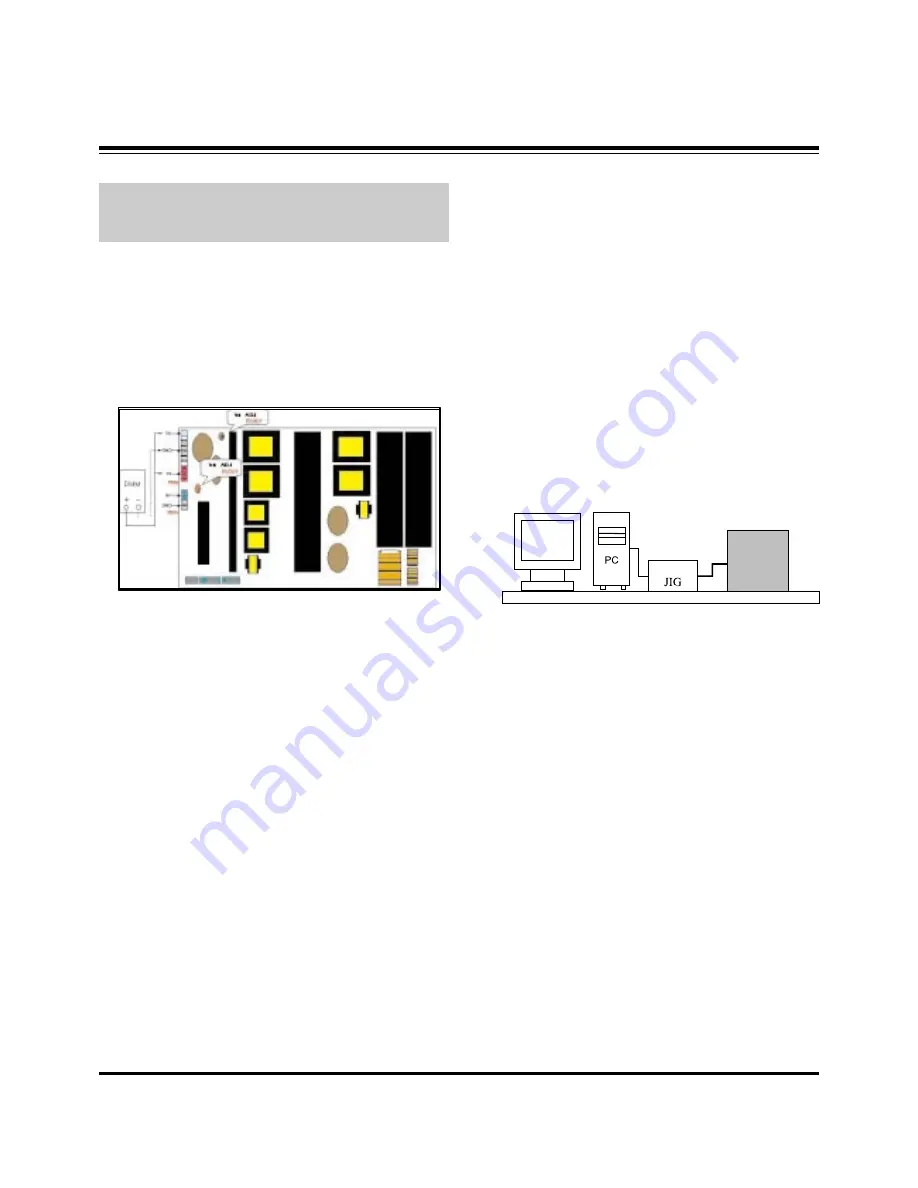
6-2. Connection Diagram for Measuring
Refer to Fig 1.
6-3. Adjustment
(1) Va Adjustment
1) C terminal of D.M.M to Va pin of P805 and
connect – terminal to GND pin of P805.
2) Adjust RV601 voltage to match that of the label on the
Top/Right of the panel. (Deviation : ±0.5V)
(2) Vs Adjustment
1) C terminal of D.M.M to Vs pin of P805 and
connect – terminal to GND pin of P805.
2) Adjust RV401 voltage to match that of the label on the
Top/Right of the panel. (Deviation : ±0.5V)
7. EDID(The Extended Display
Identification Data)/DDC
(Display Data Channel) download
This is the function that enables “Plug and Play".
7-1. HDMI EDID Data Input
(1) Required Test Equipment
1) Jig for adjusting PC, DDC. (PC serial to D-sub.
Connection equipment)
2) S/W for writing DDC(EDID data write & read)
3) D-Sub cable
4) Jig for HDMI Cable connection
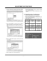
(2) Preparation for Adjustments &
Setting of Device
1) Set devices as below and turn on the PC and JIG.
2) Open S/W for writing DDC (EDID data write & read).
(operated in DOS mode)
7-2. EDID DATA for AF-05FC
:
EDID for HDMI 1 (DDC (Display Data Channel) Data)
EDID table =
0 1 2 3 4 5 6 7 8 9 A B C D E F
__________________________________________________
00 | 00 FF FF FF FF FF FF 00 1E 6D 01 00 01 01 01 01
10 | 00 0F 01 03 80 73 41 96 0A CF 74 A3 57 4C B0 23
20 | 09 48 4C 2F CE 00 31 40 45 40 61 40 01 01 01 01
30 | 01 01 01 01 01 01 01 1D 00 72 51 D0 1E 20 6E 28
40 | 55 00 C4 8E 21 00 00 1E 01 1D 80 18 71 1C 16 20
50 | 58 2C 25 00 C4 8E 21 00 00 9E 00 00 00 FC 00 4C
60 | 47 2D 54 56 0A 20 20 20 20 20 20 20 00 00 00 FD
70 | 00 3B 3C 1F 2D 08 00 0A 20 20 20 20 20 20 01 77
80 | 02 03 15 F2 46 84 85 03 02 07 06 23 15 07 50 65
90 | 03 0C 00 10 00 8C 0A D0 8A 20 E0 2D 10 10 3E 96
A0 | 00 C4 8E 21 00 00 18 8C 0A D0 8A 20 E0 2D 10 10
B0 | 3E 96 00 13 8E 21 00 00 18 8C 0A A0 14 51 F0 16
C0 | 00 26 7C 43 00 C4 8E 21 00 00 98 8C 0A A0 14 51
D0 | F0 16 00 26 7C 43 00 13 8E 21 00 00 98 00 00 00
E0 | 00 00 00 00 00 00 00 00 00 00 00 00 00 00 00 00
F0 | 00 00 00 00 00 00 00 00 00 00 00 00 00 00 00 88
Each PCB Assy must be checked by Check JIG Set before
assembly. (Especially, be careful Power PCB Assy which can
cause Damage to the PDP Module.)
<Fig. 1> Connection Diagram of Power Adjustment for the
Measuring (Power Board)
PDP TV SET
(or Digital Board)
<Fig. 2>
Summary of Contents for 42PX3DCV - Plasma Panel With TV Tuner
Page 14: ... 14 BLOCK DIAGRAM ...
Page 15: ... 15 NOTES ...
Page 29: ......
Page 30: ......
Page 31: ......
Page 32: ...DIGITAL TOP TUNER TOP TUNER BOTTOM DIGITAL BOTTOM SPDIF TOP SPDIF BOTTOM SIDE A V CONTROL ...


