background image

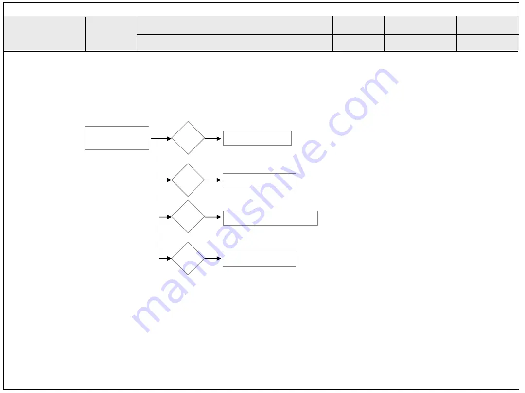
Replace module 

Zoom part with 
exterior damage 

Module 

damage 

Cabinet 

damage 

Replace cabinet 

Replace remote controller 

Remote  

controller 

damage 

Stand 

dent 

Replace stand 

F. Exterior defect


Exterior defect  

Established 

date  

Revised date  

16/16 

LCD  TV 

Error 

symptom 

Standard Repair Process 

16 

2013.01.31 

Summary of Contents for 42UB820V-ZH

Page 1: ...20V 42UB820V ZH 42UB828V 42UB828V ZH CAUTION BEFORE SERVICING THE CHASSIS READ THE SAFETY PRECAUTIONS IN THIS MANUAL LED TV SERVICE MANUAL North Latin America http aic lgservice com Europe Africa http eic lgservice com Asia Oceania http biz lgservice com Internal Use Only ...

Page 2: ...lectronics Inc All rights reserved Only for training and service purposes CONTENTS CONTENTS 2 SAFETY PRECAUTIONS 3 SERVICING PRECAUTIONS 4 SPECIFICATION 6 ADJUSTMENT INSTRUCTION 15 BLOCK DIAGRAM 23 EXPLODED VIEW 24 SCHEMATIC CIRCUIT DIAGRAM ...

Page 3: ...inals etc to be sure the set is safe to operate without damage of electrical shock Leakage Current Cold Check Antenna Cold Check With the instrument AC plug removed from AC source connect an electrical jumper across the two AC plug prongs Place the AC switch in the on position connect one lead of ohm meter to the AC plug prongs tied together and touch other ohm meter lead in turn to each exposed m...

Page 4: ...ctrostatic charge on your body by touching a known earth ground Alter natively obtain and wear a commercially available discharg ing wrist strap device which should be removed to prevent potential shock reasons prior to applying power to the unit under test 2 After removing an electrical assembly equipped with ES devices place the assembly on a conductive surface such as aluminum foil to prevent e...

Page 5: ...he solder joints of the two original leads If they are not shiny reheat them and if necessary apply additional solder Fuse and Conventional Resistor Removal Replacement 1 Clip each fuse or resistor lead at top of the circuit board hollow stake 2 Securely crimp the leads of replacement component around notch at stake top 3 Solder the connections CAUTION Maintain original spacing between the replace...

Page 6: ...ly Belgium Russia Luxemburg Greece Czech Croatia Turkey Morocco Ireland Latvia Estonia Lithuania Poland Portugal Romania Albania Bosnia Serbia Slovakia Belarus DTV MPEG2 4 DVB T2 8 countries UK Ireland Sweden Denmark Finland Norway Ukraine Kaza khstan Russia DTV MPEG2 4 DVB C 37 countries Germany Netherland Switzerland Hungary Austria Slovenia Bul garia France Spain Italy Belgium Russia Luxemburg ...

Page 7: ...l Bitrate_Mbit s 1 4 1 8 1 16 1 32 Modulation Code Rate QPSK 1 2 2 3 3 4 5 6 7 8 16 QAM 1 2 2 3 3 4 5 6 7 8 64 QAM 1 2 2 3 3 4 5 6 7 8 DVB T2 Guard Interval Bitrate_Mbit s 1 4 1 8 1 16 1 32 1 128 19 128 19 256 Modulation Code Rate QPSK 1 2 2 5 2 3 3 4 5 6 16 QAM 1 2 2 5 2 3 3 4 5 6 64 QAM 1 2 2 5 2 3 3 4 5 6 256 QAM 1 2 2 5 2 3 3 4 5 6 DVB C Symbolrate 4 0 Msymbols s to 7 2 Msymbols s Modulation 1...

Page 8: ...I 3 720 576i 15 63 50 00 13 50 SDTV DVD 576I 625I 50Hz 4 720 480p 31 47 59 94 27 00 SDTV 480P 5 720 480p 31 50 60 00 27 03 SDTV 480P 6 720 576p 31 25 50 00 27 00 SDTV 576P 50Hz 7 1280 720 44 96 59 94 74 18 HDTV 720P 8 1280 720 45 00 60 00 74 25 HDTV 720P 9 1280 720 45 00 50 00 74 25 HDTV 720P 50Hz 10 1920 1080 28 13 50 00 74 25 HDTV 1080I 50Hz 11 1920 1080 33 72 59 94 74 18 HDTV 1080I 12 1920 1080...

Page 9: ...6 1920 1080 27 00 24 00 63 36 HDTV 1080P 17 1920 1080 33 71 29 97 79 12 HDTV 1080P 18 1920 1080 33 75 30 00 79 20 HDTV 1080P 19 1920 1080 56 25 50 00 148 50 HDTV 1080P 20 1920 1080 67 43 59 94 148 35 HDTV 1080P 21 1920 1080 67 50 60 00 148 50 HDTV 1080P 22 3840 2160 53 95 23 98 297 00 UDTV 2160P 23 3840 2160 54 00 24 00 297 00 UDTV 2160P 24 3840 2160 56 25 25 00 297 00 UDTV 2160P 25 3840 2160 61 4...

Page 10: ...59 94 25 17 VESA VGA 4 800 600 37 88 60 32 40 00 VESA SVGA 5 1024 768 48 36 60 00 65 00 VESA XGA 6 1360 768 47 71 60 02 84 75 VESA WXGA 7 1152 864 54 35 60 05 80 00 VESA 8 1280 1024 63 98 60 02 109 00 SXGA 9 1920 1080 67 50 60 00 158 40 WUXGA Reduced Blanking 10 3840 2160 54 00 24 00 297 00 UDTV 2160P 11 3840 2160 56 25 25 00 297 00 UDTV 2160P 12 3840 2160 67 50 30 00 297 00 UDTV 2160P 13 4096 216...

Page 11: ... to 3D Side by Side Half Top Bottom Checker Board Row Interleaving Column Interleaving 28 12 25 00 74 25 HDTV 1080P 33 75 30 00 74 25 HDTV 1080P 67 50 60 00 148 50 HDTV 1080P 2D to 3D Side by Side Half Top Bottom Checker Board Single Frame Sequential Row Interleaving Column Interleaving 56 25 50 00 148 50 HDTV 1080P 5 3840 2160 4096 2160 53 95 23 98 297 00 HDTV 2160P 2D to 3D Top Bottom half Side ...

Page 12: ...0 4 Side by side Full HDTV 720P 75 00 50 00 148 50 19 Top and Bottom Side by side half Primary HDTV 720P Primary HDTV 720P 89 91 90 00 59 94 60 00 148 35 148 50 4 Frame packing Line alternative Primary HDTV 720P HDTV 720P 5 1920 1080 28 13 50 00 74 25 20 Frame packing Line alternative Secondary HDTV 1080I Primary HDTV 1080I 28 13 50 00 148 50 20 Side by side Full HDTV 1080I 33 72 33 75 59 94 60 00...

Page 13: ...280 720 37 50 50 00 74 25 HDTV 720P 2D to 3D Side by Side half Top Bottom 2 1280 720 45 00 60 00 74 25 HDTV 720P 2D to 3D Side by Side half Top Bottom 3 1280 720 44 96 59 94 74 18 HDTV 720P 2D to 3D Side by Side half Top Bottom 4 1920 1080 33 75 60 00 74 25 HDTV 1080I 2D to 3D Side by Side half Top Bottom 5 1920 1080 33 72 59 94 74 18 HDTV 1080I 2D to 3D Side by Side half Top Bottom 6 1920 1080 28...

Page 14: ...l clock MHz 3D input proposed mode 1 1024 768p 30 60 2D to 3D Side by Side Half Top Bottom 2 1280 720p 30 60 3 1920 1080p 30 60 4 Others 2D to 3D No Resolution H freq kHz V freq Hz Pixel clock MHz 3D input proposed mode 1 Under 320x240 2D to 3D 2 Over 320x240 2D to 3D Side by Side Half Top Bottom 6 3 USB Movie 3D 3D supported mode manually 6 6 Miracast Widi 3D supported mode manually 6 5 USB DLNA ...

Page 15: ...se of keeping module is in the circumstance of below 20 C it should be placed in the circumstance of above 15 C for 3 hours Caution When still image is displayed for a period of 20 minutes or longer Especially where W B scale is strong Digital pattern 13ch and or Cross hatch pattern 09ch there can some afterimage in the black level area 3 Automatic Adjustment 3 1 MAC address D L CI key D L Widevin...

Page 16: ...itialized Not always It is impossible to download by bar code scan so It need Manual download 1 Press the Instart key of Adjustment remote control 2 Go to the menu 7 Model Number D L like below photo 3 Input the Factory model name ex 47LB650V ZA or Serial number like photo 4 Check the model name Instart menu Factory name displayed ex 47LB650V ZA 5 Check the Diagnostics DTV country only Buyer model...

Page 17: ... 63 00 00 1E 0x07 00 00 00 00 00 00 00 00 00 00 00 00 00 00 00 ⓔ2 0 1 2 3 4 5 6 7 8 9 A B C D E F 0 00 FF FF FF FF FF FF 00 1E 6D 01 00 01 01 01 01 10 01 18 01 03 80 A0 5A 78 0A EE 91 A3 54 4C 99 26 20 0F 50 54 A1 08 00 31 40 45 40 61 40 71 40 81 80 30 01 01 01 01 01 01 02 3A 80 18 71 38 2D 40 58 2C 40 45 00 40 84 63 00 00 1E 66 21 50 B0 51 00 1B 30 50 40 70 36 00 40 84 63 00 00 1E 00 00 00 FD 00 ...

Page 18: ...te balance auto adj wb 00 10 Gain adj ja 00 ff Adj data jb 00 c0 wb 00 1f Gain adj completed wb 00 20 Start wb 00 2f end Off set adj wb 00 ff End white balance auto adj Adj Map Input FFh Checksum HDMI1 E7 2D HDMI2 E7 1D HDMI3 E7 0D 0 1 2 3 4 5 6 7 8 9 A B C D E F 80 02 03 3C F1 54 10 9F 04 13 05 14 03 02 12 20 21 90 22 15 01 5D 5E 5F 62 63 64 29 3D 06 C0 15 07 50 A0 09 57 07 6E 03 0C 00 30 00 B8 3...

Page 19: ...ark surrounding 2 Probe location Color Analyzer CA 210 probe should be within 10 cm and perpendicular of the module surface 80 100 3 Aging time After Aging Start Keep the Power ON status during 5 Minutes In case of LCD Back light on should be checked using no signal or Full white pattern 4 2 6 Reference White balance Adj coordinate and color temperature Luminance 206 Gray Standard color coordinate...

Page 20: ...ith the TV Set by select Mute OK Key on the Adjustment remote control 4 5 3D function test Pattern Generator MSHG 600 MSPG 6100 Support HDMI1 4 HDMI mode NO 872 pattern No 83 1 Please input 3D test pattern like below 2 When 3D OSD appear automatically then select green key 3 Don t wear a 3D Glasses Check the picture like below 4 6 Option selection per country 4 6 1 Overview Option selection is onl...

Page 21: ...sert 2 Perform GND Internal Pressure auto check Unit fully inserted Power cord Antenna cable and A V arrive to the auto check process Connect D terminal to AV JACK TESTER Auto CONTROLLER GWS103 4 ON Perform GND TEST If NG Buzzer will sound to inform the operator If OK changeover to I P check automatically Remove CORD A V form AV JACK BOX Perform I P test If NG Buzzer will sound to inform the opera...

Page 22: ...cally Download 3 Show the message Copying files from memory 4 Updating is starting 5 Updating Completed The TV will restart automatically 6 If your TV is turned on check your updated version and Tool option explain the Tool option next stage If downloading version is more high than your TV have TV can lost all channel data In this case you have to channel recover if all channel data is cleared you...

Page 23: ...ER T2 C A TUNER S2 DVB S DEMOD S2 LNB USB2 USB3 2 0 Video 4K 30p 2K 60p Vx1 4 lane OSD FHD 60p Vx1 2 lane eMMC 4GB Sub Micom RENESAS R5F100GEAFB DDR3 1866 X 16 512MB X 2EA P_TS X_TAL 24MHz T2 C S2 W O AD A B X_TAL 32 768KHz I2S Out I2C 4 Vx1 USB P_TS I2C 1 H P AV COMP SCART IN OUT OCP 2A OCP 1 5A HDD R E A R H CVBS YPbPr CVBS RGB SPDIF OUT ETHERNET I2C 0 IR KEY WIFI BT Combo LOGO LIGHT Ready SUB A...

Page 24: ...electrical and mechanical parts in this chassis have special safety related characteristics These parts are identified by in the Schematic Diagram and EXPLODED VIEW It is essential that these special safety parts should be replaced with the same components as recommended in this manual to prevent X RADIATION Shock Fire or other Hazards Do not modify the original design without permission of manufa...

Page 25: ...OCKN AM28 A3P HTTPDN AL28 A4M AK27 A4P AL27 EJ_RSTZ GPIO53 F5 EJ_TRSTZ GPIO54 F4 EJ_TCK GPIO55 D5 EJ_TMS GPIO56 F6 EJ_TDI GPIO57 D4 EJ_TDO GPIO58 E5 EJ_DINT GPIO59 E4 PCM2_CEN GPIO112 AG22 PCM2_IRQA GPIO113 AH22 PCM2_WAIT GPIO114 AG23 PCM2_RESET GPIO115 AH23 GPIO_PM0 GPIO10 J5 GPIO_PM2 GPIO12 R6 GPIO_PM3 GPIO13 P4 GPIO_PM4 GPIO14 N6 GPIO_PM7 GPIO17 N5 GPIO_PM8 GPIO18 J6 GPIO_PM9 GPIO19 K4 GPIO_PM1...

Page 26: ...ND_68 H20 GND_69 H21 GND_70 H22 GND_71 H23 GND_72 H24 GND_73 H25 GND_74 H26 GND_75 H27 GND_76 J7 GND_77 J8 GND_78 J9 GND_79 J10 GND_80 J11 GND_81 J12 GND_82 J13 GND_83 J14 GND_84 J15 GND_85 J16 GND_86 J17 GND_87 J18 GND_88 J19 GND_89 J20 GND_90 J21 GND_91 J22 GND_92 J23 GND_93 J24 GND_94 J25 GND_95 J26 GND_96 K7 GND_97 K8 GND_98 K9 GND_99 K12 GND_100 K13 GND_101 K14 GND_102 K15 GND_103 K16 GND_104...

Page 27: ...2 RXD1P P3 RXD2N P2 RXD2P P1 RXDCKN M3 RXDCKP M1 DDCDD_CK GPIO41 AA6 DDCDD_DA GPIO42 AB6 HOTPLUGD GPIO34 AB5 CEC GPIO5 W4 SPDIF_IN GPIO94 D10 SPDIF_OUT GPIO95 E10 LINE_IN_0L AJ2 LINE_IN_0R AJ1 LINE_IN_2L AK3 LINE_IN_2R AK1 LINE_OUT_0L AH2 LINE_OUT_0R AJ3 EAR_OUT_L AJ4 EAR_OUT_R AJ5 ARC0 Y6 AUVAG AK2 AUVRM AK4 I2S_IN_BCK GPIO92 B10 I2S_IN_SD GPIO93 C9 I2S_IN_WS GPIO91 B9 I2S_OUT_BCK GPIO98 A7 I2S_O...

Page 28: ...C434 0 1uF C435 0 1uF C436 0 1uF C437 0 1uF C462 0 1uF C456 0 1uF C453 0 1uF C461 0 1uF C466 0 1uF C455 0 1uF C460 0 1uF C465 0 1uF DDR_VTT C459 0 1uF C464 0 1uF C458 0 1uF C463 0 1uF C454 0 1uF C457 0 1uF M0_DDR_RESET_N M1_DDR_RESET_N IC100 LGE4331 A_DDR3_A0 F16 A_DDR3_A1 C16 A_DDR3_A2 E16 A_DDR3_A3 F17 A_DDR3_A4 B17 A_DDR3_A5 E17 A_DDR3_A6 A16 A_DDR3_A7 D16 A_DDR3_A8 C15 A_DDR3_A9 E15 A_DDR3_A10...

Page 29: ...N62911501 1 VIN_1 3 VIN_3 7 V7V 9 EN 10 SW_OUT2 11 SW_OUT1 12 SW_EN2 13 SW_EN1 14 NFAULT2 15 NFAULT1 16 SW_IN1 17 SW_IN2 18 BST 19 LX_1 20 LX_2 21 LX_3 22 SS 23 FB 24 COMP 25 RLIM 26 RSET1 27 RSET2 28 AGND 5 PGND_2 8 MODE SYNC 6 PGND_3 4 PGND_1 2 VIN_2 29 EP P500 SMAW200 H24S5 EAG63590902 19 24V 14 12V 9 GND 4 PDIM 2 18 24V 13 12V 8 3 5V 3 PDIM 1 17 GND 12 12V 7 3 5V 2 INV CTL 16 GND 11 12V 6 GND ...

Page 30: ...ODEL1_OPT_4 TP601 CAM_PWR_ON_CMD TP600 CAM_SLEEP CAM_SLEEP EDID_WP EDID_WP POWER_DET_1 MODEL1_OPT_3 R627 22 OPT R629 22 OPT R630 MICOM_LM14 10K MODEL1_OPT_5 R631 10K MICOM_NON_GED R626 10K MICOM_GED MODEL1_OPT_5 IC600 R5F100GEAFB 30 EAN62632101 1 P60 SCLA0 2 P61 SDAA0 3 P62 4 P63 5 P31 TI03 TO03 INTP4 6 P75 KR5 INTP9 SCK01 SCL01 7 P74 KR4 INTP8 SI01 SDA01 8 P73 KR3 SO01 9 P72 KR2 SO21 10 P71 KR1 S...

Page 31: ... 6 OUT 5 ILIM MHL_OCP C3218 0 1uF 16V L3208 BLM18PG121SN1D R3213 47K R3249 10 D3211 30V OPT R3210 4 7K R3289 100K DDC_SDA_2 5V_NORMAL MHL_DET ZD3200 5V OPT 5 1K R3212 R3229 47K C3220 1uF 10V R3255 5 1 5V_NORMAL 5 1K R3215 R3227 10K R3200 47K L3202 BLM18PG121SN1D Q3203 SI1012CR T1 GE3 S D G C3219 22uF 10V 5V_HDMI_2 SIL9617_INT I2C_SCL8 1 0V_R9531 HDMI_HPD_2 R3211 47K 3 3V_Sil9617 5V_HDMI_3 R3294 10...

Page 32: ...SHIELD C805 0 1uF 16V OPT VA802 5 6V COMP_LR_ZENER R811 470K R818 10K R810 470K R817 10K R819 12K VA803 5 6V COMP_LR_ZENER C807 1000pF 50V OPT R820 12K C806 1000pF 50V OPT C808 47pF 50V ZD806 AV2_CVBS_ZENER_ROHM ZD807 AV2_CVBS_ZENER_ROHM ZD800 COMP_ESD R802 75 ZD801 COMP_ESD R803 75 ZD803 COMP_ESD ZD802 COMP_ESD R804 75 ZD805 COMP_ESD ZD804 COMP_ESD R805 1K Q800 MMBT3906 NXP E B C R821 10K R816 10...

Page 33: ...or_ESD_UB83 MDS62110225 M910 GASKET_8 0X6 0X10 5H SMD_GASKET_for_ESD_UB83 MDS62110225 M900 GASKET_8 0X6 0X10 5H SMD_GASKET_for_ESD_UB83 MDS62110225 M904 GASKET_8 0X6 0X10 5H SMD_GASKET_for_ESD_UB83 MDS62110225 M913 GASKET_8 0X6 0X10 5H OPT MDS62110225 M912 GASKET_8 0X6 0X10 5H OPT MDS62110225 M907 GASKET_8 0X6 0X10 5H SMD_GASKET_for_ESD_UB83 MDS62110225 M911 GASKET_8 0X6 0X10 5H SMD_GASKET_for_ESD...

Page 34: ...NORMAL 5V_USB_3 C1003 10uF 10V USB_DP2 D1003 RCLAMP0502BA 5V ZD1002 OPT USB_DP3 C1002 10uF 10V ZD1001 5V OPT USB_DM2 5V_USB_2 D1004 RCLAMP0502BA USB_DM3 IC1000 BD2242G 3 EN 2 GND 4 OC 1 VIN 6 VOUT 5 ILIM R1001 4 7K USB_DM1 D1000 RCLAMP0502BA 5V_USB_1 ZD1000 5V OPT C1001 10uF 10V USB_DP1 R1002 14K 1 JK1000 3AU04S 385 ZC LG 1 2 3 4 5 JK1001 3AU04S 385 ZC LG 1 2 3 4 5 JK1002 3AU04S 385 ZC LG 1 2 3 4 ...

Page 35: ...TDN JK1100 1 TLA 6T764 LAN_TDK 1 R1 2 R2 3 R3 4 R4 5 R5 6 R6 7 R7 8 R8 12 SHIELD 9 R9 11 R11 10 R10 GND D1 YL_C D2 YL_A D3 GN_C D4 GN_A C1103 0 01uF 50V EPHY_TDP VA1103 5 5V C1101 0 01uF 50V C1102 0 1uF 16V VA1101 5 5V EPHY_RDN R1100 0 JK1100 BS R570098 LAN_UDE 1 P1 CT 2 P2 TD 3 P3 TD 4 P4 RD 5 P5 RD 6 P6 CT 7 P7 8 P8 12 SHIELD 9 9 11 P11 10 P10 GND D1 YL_C D2 YL_A D3 GN_C D4 GN_A Ethernet Block E...

Page 36: ...pF 50V I2S_AMP SPK_L C1212 22000pF 50V 24V_AMP 24V_AMP AUD_LRCH C1201 33pF 50V 3 3V_NORMAL C1214 1uF 10V C1213 22000pF 50V AUD_MASTER_CLK C1210 0 1uF 50V C1211 0 1uF 50V L1202 SP 7850_10 10uH L1205 SP 7850_10 10uH L1204 SP 7850_10 10uH L1203 SP 7850_10 10uH IC1200 NTP7514 EAN62886101 3 NC_2 2 VDD_PLL 4 GND 1 NC_1 6 DVDD 5 NC_3 7 SDATA 8 WCK 9 BCK 10 SDA 11 SCL 12 FAULT 13 MONITOR_0 14 MONITOR_1 15...

Page 37: ...P_LOUT_MAIN SIDE_HP_MUTE 3 3V_NORMAL R1404 43K 1 HP_OUT R1401 33K C1402 1uF 10V HP_OUT R1403 4 7K HP_OUT C1404 1uF 10V HP_OUT HP_ROUT_MAIN L1400 120 ohm HP_OUT BLM18PG121SN1D C1401 180pF R1402 43K 1 HP_OUT C1408 0 1uF 16V HP_OUT C1407 180pF R1405 33K HP_ROUT_AMP C1403 10pF 50V HP_OUT C1405 10pF 50V HP_OUT IC1400 TPA6138A2 3 OUTR 2 INR 4 GND_1 1 INR 6 VSS 5 MUTE 7 CN 8 CP 9 VDD 10 GND_2 11 UVP 12 O...

Page 38: ...P 2 5TRG1 EAN61387601 TU_Q N M W 3 VIN 2 EN 4 VCTRL 1 PG 5 NC 6 VOUT 7 ADJ 8 GND 9 EP C1514 1uF TU_Q N M W R1520 10K TU_Q N M W 0 1uF C1515 TU_Q N M W C1516 10uF 10V TU_Q N M W C1513 0 1uF 16V TU_Q N M W R1521 10K 1 16W 1 TU_1 2V R1521 1 18K 1 16W 1 TU_1 1V R1522 10K 1 16W 1 TU_1 2V R1522 1 15K 1 16W 1 TU_1 1V R1502 0 FE_DEMOD1_1 R1501 0 FE_DEMOD1_1 C1504 15pF 50V OPT C1502 15pF 50V OPT R1511 33 R...

Page 39: ...47 SHIELD B1 B1 A1 A1 TU1605 TDJM C351D DEV_TDJM_C351D 1 B1 3 3V 2 RF_SW_CTL 3 NC_1 4 SCL_RF 5 SDA_RF 6 NC_2 7 NC_3 8 SIF 9 CVBS 10 NC_4 11 NC_5 12 ERROR 13 GND_1 14 MCLK 15 SYNC 16 VAILD 17 D0 18 D1 19 D2 20 D3 21 D4 22 D5 23 D6 24 D7 25 RESET_DEMOD 26 B2 3 3V 27 SCL_DEMOD 28 B3 1 1V 29 NC_6 30 SDA_DEMOD 47 SHIELD B1 B1 A1 A1 TU1601 TDJM G255D DEV_TDJM_G255D 1 B1 3 3V 2 NC_1 3 NC_2 4 SCL_RF 5 SDA...

Page 40: ...HONE SOC_RX ZD1701 20V ADUC 20S 02 010L OPT C1702 0 1uF RS232C_PHONE C1700 0 33uF RS232C_PHONE SOC_TX ZD1700 ADUC 20S 02 010L 20V OPT C1704 0 1uF RS232C_PHONE C1701 0 1uF RS232C_PHONE R1700 100 RS232C_PHONE L1700 BLM18PG121SN1D HP_OUT R1705 100 1 16W 5 HP_OUT R1706 10K HP_OUT C1707 0 22uF 10V HP_OUT 3 3V_NORMAL L1701 BLM18PG121SN1D HP_OUT R1704 150 1 10W 5 HP_OUT C1706 0 22uF 10V HP_OUT R1703 150 ...

Page 41: ...W 1 LNB A_GND D1803 40V LNB_SMAB34 D1804 40V LNB_SMAB34 LNB_TX C1804 0 1uF 50V LNB C1808 0 1uF LNB C1809 10uF 25V LNB C1812 0 1uF LNB C1802 0 22uF 25V LNB I2C_SCL2 C1800 18pF LNB C1801 33pF LNB IC1800 A8303SESTR T LNB EAN62653701 1 VCP 3 NC_1 7 SCL 9 ADD 10 TONECTRL 11 TCAP 12 ISET 13 VREG 14 GND 15 VIN 16 LX 17 GNDLX 18 NC_2 19 NC_3 20 BOOST 5 TDO 8 SDA 6 IRQ 4 TDI 2 LNB 21 EP GND D1801 1 30V SS2...

Page 42: ..._4 P3 VCCQ_5 P5 VCC_1 E6 VCC_2 F5 VCC_3 J10 VCC_4 K9 VDDI C2 VSS_1 E7 VSS_2 G5 VSS_3 H10 VSS_4 K8 VSSQ_1 C4 VSSQ_2 N2 VSSQ_3 N5 VSSQ_4 P4 VSSQ_5 P6 NC_1 A1 NC_2 A2 NC_3 A8 NC_4 A9 NC_5 A10 NC_6 A11 NC_7 A12 NC_8 A13 NC_9 A14 NC_10 B1 NC_11 B7 NC_12 B8 NC_13 B9 NC_14 B10 NC_15 B11 NC_16 B12 NC_17 B13 NC_18 B14 NC_19 C1 NC_20 C3 NC_22 C7 NC_23 C8 NC_24 C9 NC_25 C10 NC_26 C11 NC_27 C12 NC_28 C13 NC_2...

Page 43: ...0 470K EU R2103 10K EU R2110 12K EU R2104 10K EU R2101 470K EU R2111 12K EU R2106 75 EU R2109 75 EU R2107 75 EU R2116 1K 1 16W 5 EU R2105 75 3216 EU CVBS_OUT_SEL R2118 10K EU_CVBSOUT Q2100 2SC3052 EU_CVBSOUT E B C 3 3V_NORMAL L2100 BLM18PG121SN1D EU_CVBSOUT 3 3V_CVBS_out R2119 1 8K EU_CVBSOUT Q2101 RTR030P02 EU_CVBSOUT S D G C2108 1uF OPT R2120 1K OPT 3 3V_CVBS_out Q2103 RTR030P02 EU_CVBSOUT S D G...

Page 44: ... 470K OPT C2209 6800pF OPT IC2200 AZ4580MTR E1 EU 3 IN1 2 IN1 4 VEE 1 OUT1 5 IN2 6 IN2 7 OUT2 8 VCC DTV MNT_R_OUT R2204 33K EU C2208 33pF EU Q2201 MMBT3904 NXP EU E B C Q2202 1 PDTA114ET EU_SCART_MUTE_NXP E B C 12V R2211 2 2K EU R2200 10K EU SCART_AMP_R_FB R2201 10K EU SCART_AMP_L_FB R2214 5 6K EU R2215 220K EU C2211 330pF EU R2216 5 6K EU R2217 220K EU C2212 330pF EU SCART_Rout C2202 10uF EU C221...

Page 45: ..._MDI 7 AR2309 33 CI_IORD C2300 2pF 50V R2309 10K EB_ADDR 11 EB_ADDR 14 CAM_IREQ_N CI_MDI 2 CI_OE CI_MIVAL_ERR CI_MDI 0 REG CI_ADDR 0 14 CI_CD1 CI_MDI 2 EB_ADDR 1 REG TPI_SOP 5V_NORMAL EB_ADDR 4 R2306 33 C2303 10uF 10V EB_ADDR 12 CI_ADDR 12 CI_MISTRT AR2303 33 CI_MCLKI EB_ADDR 9 IC2300 74LVC1G32GW OR_GATE_CI_PHILIPS 3 GND 2 A 4 Y 1 B 5 VCC TPI_CLK C2301 0 1uF GND CI_ADDR 10 AR2307 33 AR2304 33 CI_I...

Page 46: ... C13303 0 1uF 16V C13022 0 1uF TXDAP4_L R12901 0 Non_UB95 GND_Vx1 IC2500 LGE7411 URSA9 RB0N AG2 RB0P AG1 RB1N AH3 RB1P AH1 RB2N AH2 RB2P AJ3 RBCKN AJ2 RBCKP AK2 RB3N AK1 RB3P AL1 RB4N AM2 RB4P AL2 RC0N AK3 RC0P AL3 RC1N AK4 RC1P AL4 RC2N AM4 RC2P AK5 RCCKN AM5 RCCKP AL5 RC3N AK6 RC3P AL6 RC4N AK7 RC4P AL7 RD0N AM7 RD0P AK8 RD1N AM8 RD1P AL8 RD2N AK9 RD2P AL9 RDCKN AK10 RDCKP AL10 RD3N AM10 RD3P AK...

Page 47: ...10K OPT TXDAN2_L R220 0 OPT TXDAP5_L GND_Vx1_2 TXDBN11_L R13041 10K LGD_Module R13055 33 OPT 3 3V_NORMAL R13059 33 OPT TXDBN2_L TXDBP6_L R221 0 URSA_TX_HTPD_Pullup TXDBN8_L R13063 1 5K R222 10K URSA_TX_HTPD_Pullup TXDBN7_L R211 1 5K URSA_TX_HTPD_Pullup TXDBP0_L 1 8V HTPDn_IN TXDBP1_L TXDAN4_L LOCKn_IN L13000 MLB 201209 0120P N2 51pin_12V TXDAN7_L L13001 BLM18PG121SN1D OLED R13037 0 Non_AUO_Module ...

Page 48: ...6 0 1uF 16V C13151 0 1uF 16V A_DDR3_A 8 A_DDR3_CKE A_DDR3_A 0 B_DDR3_DQS3B A_DDR3_A 15 1 5V_U_DDR A_DDR3_DQS2B C13150 4700pF DDR_VTT_URSA_0 A_DDR3_A 10 B_DDR3_A 4 1 5V_U_DDR A_DDR3_A 13 DDR_VTT_URSA A_DDR3_A 7 A_DDR3_A 6 B_DDR3_BA 2 R13103 1K B_DDR3_CASZ 1 5V_U_DDR B_DDR3_A 0 A_DDR3_DQS2 A_DDR3_A 15 B_DDR3_A 8 C13232 0 1uF 16V C13204 0 1uF 16V A_DDR3_DM3 A_DDR3_DM3 B_DDR3_DM0 B_DDR3_A 11 A_DDR3_A ...

Page 49: ...16 F5 NC_17 M5 NC_18 M6 NC_19 M7 NC_20 N5 NC_21 R7 NC_22 P7 NC_23 N7 NC_24 N6 I2C_HSC_SDA VSYNC_LIKE2 AG25 I2C_HSC_SCL VSYNC_LIKE3 AH25 SPI1_CK PWM2 GPIO58 AH28 SPI1_DI PWM3 GPIO59 AJ27 SPI2_CK PWM0 GPIO56 AJ29 SPI2_DI PWM1 GPIO57 AF27 SPI3_CK DIM10 GPIO54 AG28 SPI3_DI DIM11 GPIO55 AH27 SPI4_CK DIM8 GPIO52 AG27 SPI4_DI DIM9 GPIO53 AG26 VSYNC_LIKE PWM5 GPIO40 AF28 DIM0 GPIO 32 AG23 DIM1 GPIO 33 AG2...

Page 50: ...VSS_202 AJ13 VSS_203 G14 VSS_204 H14 VSS_205 J14 VSS_206 K14 VSS_207 L14 VSS_208 P14 VSS_209 R14 VSS_210 T14 VSS_211 U14 VSS_212 V14 VSS_213 W14 VSS_214 Y14 VSS_215 AA14 VSS_216 AB14 VSS_217 AE14 VSS_218 AF14 VSS_219 AG14 VSS_220 AH14 VSS_221 AJ14 VSS_222 A15 VSS_223 B15 VSS_224 D15 VSS_225 G15 VSS_226 H15 VSS_227 J15 VSS_228 K15 VSS_229 L15 VSS_230 M15 VSS_231 N15 VSS_232 P15 VSS_233 R15 VSS_234 ...

Page 51: ... 1uF 16V R13406 91K 1 16W 1 C13446 2200pF 50V 1 0V_DCDC_ROHM R13403 4 7 C13411 22uF C13400 22uF C13440 10uF 25V OPT 12V ZD13400 2 5V OPT R13421 18K 1 C13445 1uF 10V C13406 2200pF 50V C13409 10uF 16V R13402 3 3 1 10W 5 C13434 10uF 25V TCON_PWR_5pin_Wafer R13405 27K 1 16W 1 C13446 1 3300pF 50V 1 0V_DCDC_TI C13407 1uF 10V R13407 39K 1 16W 5 R13404 10K VDDC R13424 10K L13402 C13404 470pF 50V C13402 0 ...

Page 52: ......

Page 53: ...r 5 6 B Power error No power 6 7 Off when on off while viewing power auto on off 7 8 C Audio error No audio Normal video 8 9 Wrecked audio discontinuation noise 9 10 D Function error Remote control Local switch checking 10 MR Magic Remocon operating checking 11 11 12 Wifi operating checking 12 13 External device recognition error 13 145 E Noise Circuit noise mechanical noise 14 15 F Exterior error...

Page 54: ...lace Inverter or module N Repair Power Board or parts End Always check record S W Version and White Balance value before replacing the Main Board Replace Main Board Re enter White Balance value Precaution Established date Standard Repair Process Revised date 1 16 LCD TV Error symptom A Video error No video Normal audio A18 A1 A18 A4 A2 First of all Check whether all of cables between board is inse...

Page 55: ...r Board 3 5V 12V 20V or 24V No Video No audio Check and replace MAIN B D Y Replace Power Board and repair parts N End Standard Repair Process A Video error No video No audio A18 Established date Revised date 2 16 LCD TV Error symptom 2 2013 01 31 ...

Page 56: ...t Top Box Different maker TV etc SVC Bulletin Replace Main B D Check Tuner soldering Normal Picture Y N Y Close Y Close By using Digital signal level meter By using Diagnostics menu on OSD Setting Support Signal Test Signal strength Normal over 50 Signal Quality Normal over 50 Normal Picture Y Contact with signal distributor or broadcaster Cable or Air N Normal Picture Y Close N A4 Standard Repair...

Page 57: ... normal External Input Component error Check external device and cable Y External device Cable normal HDMI error Check external device and cable Replace Main T con B D Replace Main T con B D N N A Video error Color error A6 N Y End Replace module Request repair for external device cable Color error Check Test pattern A8 A7 Standard Repair Process Established date Revised date 4 16 LCD TV Error sym...

Page 58: ...n of External Input Component RGB and HDMI DVI by connecting Jig pattern Generator Set top Box etc N Y Replace Main T con B D Screen normal Check screen condition by input External Input Component HDMI DVI Request repair for external device Component error HDMI DVI Connect other external device and cable Check normal operation of External Input Component RGB and HDMI DVI by connecting Jig pattern ...

Page 59: ...eck Logo LED Replace Power B D Measure voltage of each output of Power B D N Y Normal voltage Replace Main B D Y OK Replace Main B D N Y Normal Check ST BY 3 5V Replace Power B D N Y Normal voltage Replace Power B D Y A17 A18 A18 A18 Standard Repair Process Established date Revised date 6 16 LCD TV Error symptom 6 Stand By Red or Turn On Operating Turn Off Close 2013 01 31 ...

Page 60: ...off List Explanation Normal POWEROFF_REMOTEKEY Power off by REMOTE CONTROL POWEROFF_OFFTIMER Power off by OFF TIMER POWEROFF_SLEEPTIMER Power off by SLEEP TIMER POWEROFF_INSTOP Power off by INSTOP KEY POWEROFF_AUTOOFF Power off by AUTO OFF POWEROFF_ONTIMER Power off by ON TIMER POWEROFF_RS232C Power off by RS232C POWEROFF_RESREC Power off by Reservated Record POWEROFF_RECEND Power off by End of Re...

Page 61: ...Power Board Normal voltage Y N Replace Power Board and repair parts Check Speaker disconnection N Y Replace Speaker Replace MAIN Board End C Audio error No audio Normal video A20 A21 A18 Disconnection Established date Revised date 8 16 LCD TV Error symptom Standard Repair Process 8 2013 01 31 ...

Page 62: ...dio Discontinuation Noise only for External Input Connect and check other external device N Y Normal audio Check and fix external device Replace Power B D N Y Normal voltage Check input signal RF External Input signal Signal normal When RF signal is not received Request repair to external cable ANT provider Y Check audio B Voltage 24V Replace Main B D In case of External Input signal error Check a...

Page 63: ...erating When turn off light in room Check Replace Baterry of R C Check Repair Cable connection Connector solder Normal operating Check B 3 5V On Main B D A22 Normal Voltage Close N N Check 3 5v on Power B D Replace Power B D or Replace Main B D Power B D don t have problem A18 Check IR Output signal Normal Signal N Y Repair Replace IR B D N A22 Replace Main B D Y A22 Standard Repair Process Establ...

Page 64: ...N Y Standard Repair Process Established date Revised date 11 16 LCD TV Error symptom 11 Replace MR Turn off on the set and press the wheel Press the back key about 5sec Close If you conduct the loop at 3times change the M4 Y Check the INSTART menu RF Receiver ver is 00 00 Y Check Repair RF assy connection N Down load the Firmware INSTART MENU 14 RF Remocon Test 3 Firmware download Y RF Receiver ve...

Page 65: ...i Fi Mac value is NG Y Check Repair Wifi cable connection N Check the Wifi wafer 1pin Standard Repair Process Established date Revised date 12 16 LCD TV Error symptom 12 Change the Wifi assy Normal Voltage Close Y Y N Replace Main B D Wi Fi Mac value is NG N Close A24 A4 A4 A24 2013 01 31 ...

Page 66: ...put and Component Recognition error Check and fix external device cable HDMI DVI Optical Recognition error Replace Main B D Replace Main B D Fix in accordance with technical information D Function error External device recognition error Established date Revised date 14 16 LCD TV Error symptom Standard Repair Process 14 2013 01 31 ...

Page 67: ...e KMS fix information and then proceed as shown in the solution manual For models without any fix information provide the description Mechanical noise is a natural phenomenon and apply the 1st level description When the customer does not agree apply the process by stage Describe the basis of the description in Part related to nose in the Owner s Manual E Noise Circuit noise mechanical noise Establ...

Page 68: ...odule damage Cabinet damage Replace cabinet Replace remote controller Remote controller damage Stand dent Replace stand F Exterior defect Exterior defect Established date Revised date 16 16 LCD TV Error symptom Standard Repair Process 16 2013 01 31 ...

Page 69: ...A3 5 LCD TV Version checking method A4 6 Tuner Checking Part A5 7 A Video error _Vertical Horizontal bar residual image light spot LCD TV connection diagram A6 8 A Video error_ Color error Check Link Cable EPI reconnection condition A7 9 Adjustment Test pattern ADJ Key A8 10 Appendix Defected Type caused by T Con Inverter Module Exchange Main Board 1 A 1 5 11 Exchange Main Board 2 A 2 5 12 Exchang...

Page 70: ... OFF MODE checking method A19 19 C Audio error_ No audio Normal video Checking method in menu when there is no audio A20 20 Voltage and speaker checking method when there is no audio A21 21 D Function error Remote controller operation checking method A22 22 Motion Remote operation checking method A23 23 Wifi operation checking method A24 24 Camera operation checking method A25 Not Used 25 E Etc To...

Page 71: ... Error symptom Content Check LCD back light with naked eye A Video error_No video Normal audio After turning on the power and disassembling the case check with the naked eye whether you can see light from locations LCD TV A1 2013 01 31 XXUB83 820X XX Tuner is different from region ...

Page 72: ... for adjustment 2 Enter into White Balance of item 6 3 After recording the R G B GAIN Cut value of Color Temp Cool Medium Warm re enter the value after replacing the MAIN BOARD Entry method 1 Press the ADJ button on the remote controller for adjustment 2 Enter into White Balance of item 10 3 After recording the R G B GAIN Cut value of Color Temp Cool Medium Warm re enter the value after replacing ...

Page 73: ...rong use the attenuator 10dB 15dB 20dB etc Standard Repair Process Detail Technical Manual TUNER input signal strength checking method A Video error_Video error video lag stop ALL MODELS A3 Established date Revised date Error symptom Content LCD TV A3 2014 02 14 ...

Page 74: ...hecking method A Video error_Video error video lag stop 1 Checking method for remote controller for adjustment Press the IN START with the remote controller for adjustment Version ALL MODELS A4 Established date Revised date Error symptom Content LCD TV A4 2014 02 14 ...

Page 75: ...al device is connected 2 After measuring each voltage from power supply finally replace the MAIN BOARD Standard Repair Process Detail Technical Manual TUNER checking part A Video error_Video error video lag stop ALL MODELS A5 Established date Revised date Error symptom Content LCD TV A5 2014 02 14 ...

Page 76: ... connection diagram 1 A Video error _Vertical Horizontal bar residual image light spot As the part connecting to the external input check the screen condition by signal A6 Established date Revised date Error symptom Content LCD TV A6 ALL MODELS 2014 02 14 ...

Page 77: ...k Cable LVDS reconnection condition A Video error_Color error Check the contact condition of the Link Cable especially dust or mis insertion A7 Established date Revised date Error symptom Content LCD TV A7 ALL MODELS 2014 02 14 Tuner is different from region ...

Page 78: ... Video error_Color error You can view 6 types of patterns using the ADJ Key Checking item 1 Defective pixel 2 Residual image 3 MODULE error ADD BAR SCAN BAR 4 Video error Classification of MODULE or Main B D A8 Established date Revised date Error symptom Content LCD TV A8 2014 02 14 ...

Page 79: ... Broken T Con Defect CNT Broken Solder defect CNT Broken Solder defect CNT Broken Solder defect CNT Broken Solder defect CNT Broken Abnormal Power Section Solder defect Short Crack Abnormal Power Section Solder defect Short Crack Appendix Exchange Main Board 1 A 1 5 ...

Page 80: ...rmal Power Section Solder defect Short Crack Abnormal Power Section Solder defect Short Crack Fuse Open Abnormal power section Noise GRADATION GRADATION Abnormal Display Appendix Exchange Main Board 2 A 2 5 ...

Page 81: ...Appendix Exchange Power Board PSU No Light Dim Light Dim Light Dim Light No picture Sound Ok A 3 5 ...

Page 82: ...pendix Exchange the Module 1 Panel Mura Light leakage Press damage Crosstalk Crosstalk Press damage Panel Mura Light leakage Press damage A 4 5 Un repairable Cases In this case please exchange the module ...

Page 83: ...C Defect Vertical Line Source TAB IC Defect Vertical Block Source TAB IC Defect Horizontal Block Gate TAB IC Defect Horizontal line Gate TAB IC Defect Gate TAB IC Defect Horizontal Block Gate TAB IC Defect Appendix Exchange the Module 2 A 5 5 Un repairable Cases In this case please exchange the module ...

Page 84: ...s Detail Technical Manual Check front Power Indicator B Power error _No power A17 Established date Revised date Error symptom Content LCD TV A17 ST BY condition On or Off Power ON condition Turn Off 2014 02 07 XXUB83 820X XX ...

Page 85: ... 5V B Power error _No power LCD TV A18 Check the DC 24V 12V 3 5V 2014 02 05 1 PWR ON 2 DVR_ON 3 P_DIM 1 4 PDIM 2 5 3 5V 6 GND 7 3 5V 8 3 5V 9 GND 10 GND 11 12V 12 12V 13 12V 14 12V 15 12V 16 GND 17 GND 18 24V 19 24V 20 24V 21 24V 22 24V 23 GND 24 GND 25 SCLK 26 GND 27 SIN 28 VSYNC P_main Maker Yeonho 28Pin SMAW200 H28S5K 14년 적용 28Pin map LPB ...

Page 86: ...or adjustment 2 Check the entry into adjustment item 3 Standard Repair Process Detail Technical Manual POWER OFF MODE checking method B Power error _Off when on off whiling viewing ALL MODELS A19 Established date Revised date Error symptom Content LCD TV A19 2014 02 05 ...

Page 87: ... function of the Menu 3 Select the Sound Out 4 Select TV Speaker Standard Repair Process Detail Technical Manual Checking method in menu when there is no audio C Audio error_No audio Normal video A20 Established date Revised date Error symptom Content LCD TV A20 2014 02 05 XXUB83 820X XX ...

Page 88: ...he GND and output terminal the speaker is normal Standard Repair Process Detail Technical Manual Voltage and speaker checking method when there is no audio C Audio error_No audio Normal video A21 Established date Revised date Error symptom Content LCD TV A21 2014 02 05 1 PWR ON 2 DVR_ON 3 P_DIM 1 4 PDIM 2 5 3 5V 6 GND 7 3 5V 8 3 5V 9 GND 10 GND 11 12V 12 12V 13 12V 14 12V 15 12V 16 GND 17 GND 18 2...

Page 89: ...e slowly otherwise it s defective Standard Repair Process Detail Technical Manual Remote controller operation checking method D Function error A22 Established date Revised date Error symptom Content LCD TV A22 2014 02 07 1 GND 2 3 5V WOL 3 BT_RESET 4 USB_DM 5 NC 6 USB_DP 7 WOL 8 GND 9 SDA 10 GND 11 SCL 12 KEY1 13 GND 14 KEY2 15 IR 16 3 5V_ST 17 LED_R 18 GND Checking order to check remote controlle...

Page 90: ...l Motion Remote Wifi operation checking method Established date Revised date Error symptom Content LCD TV A23 A23 D Function error 2014 02 07 1 GND 2 3 5V WOL 3 BT_RESET 4 USB_DM 5 NC 6 USB_DP 7 WOL 8 GND 9 SDA 10 GND 11 SCL 12 KEY1 13 GND 14 KEY2 15 IR 16 3 5V_ST 17 LED_R 18 GND Checking order to check motion remote wifi Front Back Wifi BT Combo XXUB83 820X XX ...

Reviews: