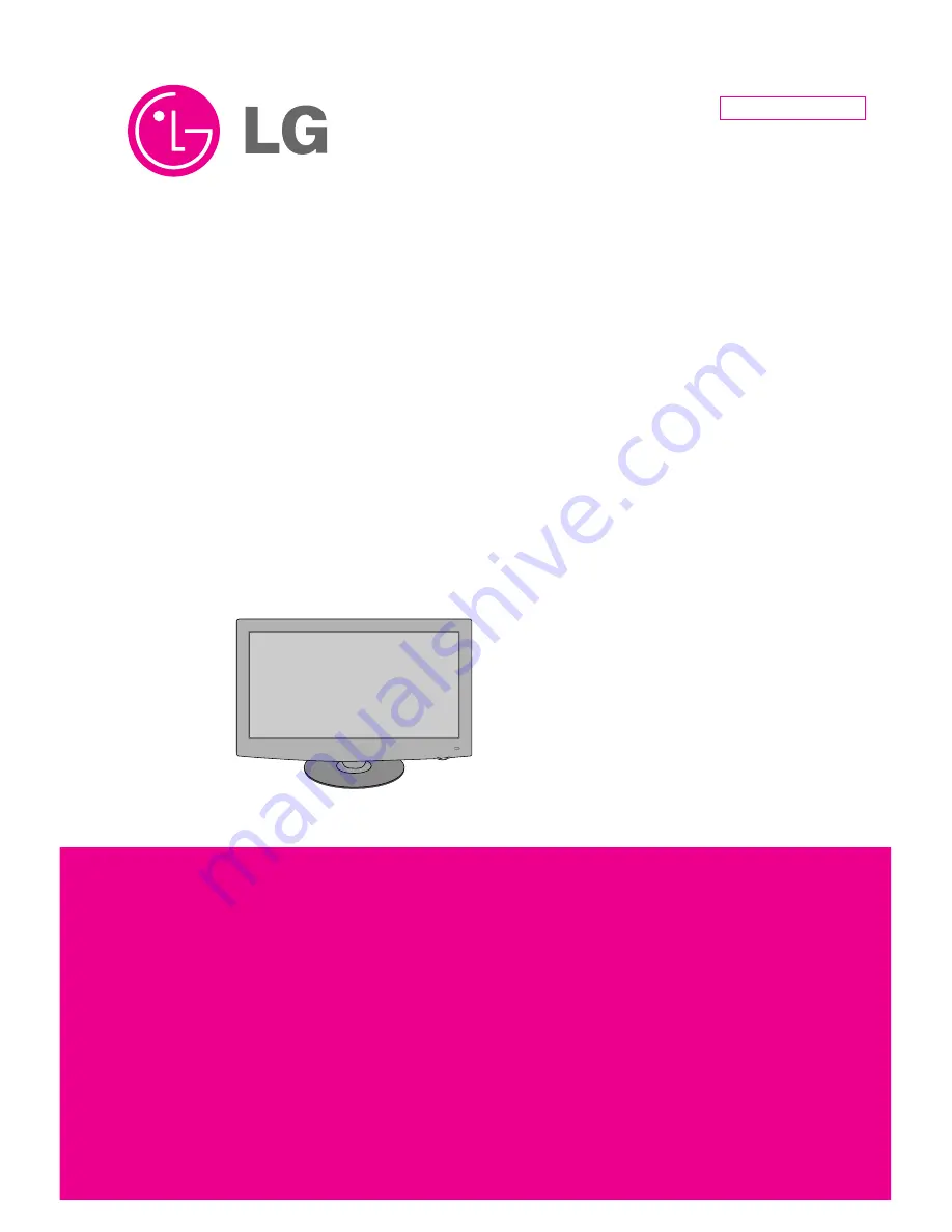
LCD TV
SERVICE MANUAL
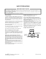
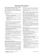
CAUTION
BEFORE SERVICING THE CHASSIS,
READ THE SAFETY PRECAUTIONS IN THIS MANUAL.
CHASSIS : LA92C
MODEL : 47LH90
47LH90-UB
North/Latin America
http://aic.lgservice.com
Europe/Africa
http://eic.lgservice.com
Asia/Oceania
http://biz.lgservice.com
Internal Use Only
Printed in Korea
P/NO : MFL58600434 (0904-REV00)
Summary of Contents for 47LH90 Series
Page 52: ......


