


X2
50Mhz
50PS60 TV INTERCONNECT DIAGRAM
Switch Mode Power Supply
P812
F101-2
SC101
15A / 250V
P813
P811
P811 / P812 “SMPS”
P114
Floating
Gnd
P814
Control PWB
P101
P1
Pin
Label
STBY
Run Diode
Check
1,2
VS
0V
195V
Gnd
NC
3
4,5
6,7
8
9,10
0V
Open
0.86V
NC
VA
M5V
NC
Gnd
0V
Gnd
Open
5.0V
NC
Gnd
65V
IC1
P5
P104
P2
P200
P101
P102
IC306
P202
P3
AUTO GEN
P301
P103
P106
P104
P102
P105
P214
P116
P216
Floating
GND
P312
Floating
GND
P314
Floating
GND
P311
P313
P101
P307
P111
P211
P112
P309
P101
P102
P103
P104
P201
P202
P203
P204
Odd
Waveform
Even
Waveform
VSC TP (-)
(-) (+)
R306
R305
Even
Waveform
Odd
Waveform
VSCAN
SET-Dn1
DD_Var (-VY)
SET-Up1
IC7
IC12
IC304
IC16
FS901 5V
4A 125V
FS303 VA
10A 125V
FS302 VS
3A 250V
N/C
n/c
N/C
N/C
P100
(+)VZB TP
R457
VZB
(-)VZB TP
FS100 5V
4A 125V
VR601
VR902
VR602
VR901
VR201
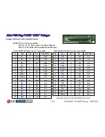
Pin
Label
STBY
Run Diode
Check
1,2,3,4
0V
5V
5,6,7,8
0.75V
5V
P813 “SMPS” - P200 “CONTROL”
IC7
1 (0V)
2 (3.3V)
3 (5.0V)
IC12
1 (0V)
2 (2.5V)
3 (5.0V)
IC304
1 (0V)
2 (3.3V)
3 (5.0V)
SMPS TEST
: Removing connector P814 will force the SMPS into full run mode.
Only do this with AC power removed then reapply AC power.
Q93
Q94
Q95
Q96
Q97
Q98
Q99
Q73
Q81
Q82
Q83
Q72
Q
71
D72
D74
D52
Q51
Q52
Q61
D
51
Q62
D61
D62
Q11
Q12
D16
D17
D31
Q30
Q31
Q40
D
30
Q41
D40
D41
Q10
Q22
Q21
Q20
D7
D6
P6
VA Adj
VS Adj
Fl103
Z-SUS TP
FS102 VS
3A 250V
P121
IC16
7
1 (0V)
2 (3.3V)
3 (5.0V)
Q1
5
Q1
4
Q1
3
AUTO GEN
is activated by
shorting pin 1 to pin 2 of
connector P6. Note: The
LVDS cable must be removed
for Auto Gen to work.
P814 “SMPS” - P1108 “MAIN”
*If pin 24 is at 4.3V with the unit is in standby the Power
Button is released and will prevent the unit from coming on.
P100 “Z-SUS” - P2 “Control”
Z-SUS LOCATION
Generic Part
D16, 17
D30, 31, 40, 41
RF2001
45F122
Q10, 11, 12, 20, 21, 22, 30, 31, 40, 41
MA3DF30
Q13, 14
20NF20
Q15
51N25
Pin 1-4 is 3.3V to
TCP from IC304
50Mhz TP
*FL5
5V
Complete testing of the SMPS requires that you load VS
with 2 100 watt light bulbs with P811 and P812
unplugged to verify it is functioning correctly.
TIP:
If A/C DET is low or missing, Remove AC Det (pin 28) out of P814 and
jump it to any pin carrying 5V STBY. Then reapply power to the unit. If the
TV now stays on, suspect a defective SMPS.
The 17.8V on pins 1 ~ 4 is
derived by the Y-SUS PWB.
Voltages are reference to floating ground.
T901
T902
VR901
VR501
D902
D903
D911
(VSC)
Pins 1 ~ 6
are 17.8V
from Y-Sus
P1
IC904
Q901
IC909
IC908
ZD902
Q903
* FL4 / FL5:
These EMI filters have 4
solder tack points the
center two are tied to
ground.
F801
4A 250V
F302
1A 250V
Pins 1 ~ 4 are
labed as 15V
but measures
17.8V.
P100
IC902
IC903
S G
D
S
G
D
A
A
C
C
A
A
C
C
C
D904
D914
ZD1
4.7V
J1
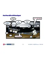
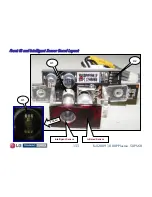
Front PWB
IR Receiver
Power Button
J2
Side (Key) Controls
P1
These voltages are reference to floating GND.
LOC
Developes
D902
+Vy
D903
D911
D912
Vsc
D914
ZD902
LOC
Pin 1
Pin 2
IC902
9V
8V
IC903
17.9V
IC904
IC905
IC908
23.3V
IC909
2.1V
10.5V
1V
0V
0V
0V
Pin 3
Cold Gnd
7.7V
5V
15.2V
5.0V
1.8V cg
.08V cg
N/A
N/A
N/A
N/A
Pin 4
0V
Y-SUS LOCATION
Generic Part
D51, 52, 61, 62, 71, 72
Q98, 99
Q93, 94, 95, 96, 97
IRFI14229
MA3DF30
45F122
K3667
Q51, 52, 61, 62, 71, 72, 73, 81, 82, 83
3
4 ~ 5
6 ~ 12
Pin
Run V Diode Chk
1 ~ 2 140V
Open
Open
nc
nc
F Gnd
FG5V
F Gnd
P116
P214
Pin
1 ~ 7
8 ~ 9
10
11 ~ 12
Run V
140V
nc
FG5V
F Gnd
Diode Chk
nc
F Gnd
Open
Open
Diode test is reference to floating GND (F Gnd)
NOTE:
Diode tests are conducted with the PWB disconnected.
P307 Y-SUS
*Generic parts list for sub supplies
located in and above Y-SUS.
10
Pin
Label
Run Diode
Check
1~4
15V
17.8V
5
ER-DN
2.2V
6
7
8
Gnd
9
Gnd
SUS-UP
11
1.49V
Gnd
Gnd
Gnd
.5V
ER-UP
Z Bias
Gnd
Gnd
1.8V
1.2V
0V
0V
Gnd
3.0V
Gnd
0.4V
SUS-DN
12
.5V
0.7V
13,14,15
Open
Pin
Label
STBY
Run Diode
Check
1,2
17V
0V
17V
3,4
Open
5,6
7,8
9,10, 12
5V
11
NC
16
17
0V
2.2V
1.2V
NC
1.45V
12V
5V STBY
5V DET
0V
0.5V
5V
Open
18
5V
1.45V
A/C DET
NC
4.7V
12V
5V
5V
5V
NC
RL ON
19
VS ON
20
21
0V
Open
Open
M5V ON
0V
Open
22
0V
Open
AUTO GND
0V
3.3V
3.3V
0V
3.2V
23
5V
Open
STBY 5
*24
*0V
KEY ON
5.0V
*0V
8 ~ 9
10
11~12
Pin
Run V Diode Chk
1 ~ 7
P313
P311
Pin
Run V
140V
nc
5V
F Gnd
Diode Chk
nc
F Gnd
1.3V
2.7V
NC
NC
NC
NC
Gnd
Gnd
Gnd
Gnd
Gnd
Gnd
Gnd
Gnd
Gnd
Gnd
Gnd
Gnd
Gnd
Gnd
Gnd
Gnd
P302
3
4 ~ 5
6 ~ 12
1 ~ 2
140V
nc
FG5V
F Gnd
2.7V
nc
1.3V
F Gnd
Diode Check
Pin
Run
1,2,3,4
VA Voltage
5
Open
nc
nc
6,7
Gnd
Gnd
Pin
Run Diode
Check
1,2,3,4
VA Voltage
5
Open
nc
nc
6,7
Gnd
Gnd
Diode Check
1.48V
1.48V
1.48V
1.48V
1.48V
Gnd
Pin
1
2
3
4
5
6
1.48V
1.4V
1.32V
7
8
9~12
Note: P2 pins
reversed from P100
LOC Source Gate
Q901
140V
144V
Q903
85V
Drain
163V
275V
88V
TIP:
To Test Z-SUS
Without a good Y-SUS.
1) Light bulb load Vs.
2) Jump the 17V from pin 1 or
pin 2 P814 to the Z-SUS
connector P100 1~5.
Note: The 17V supply will pulsate 2 to 3 times a second with Vs unloaded.
1~ 2 pins Y-Drive
Logic Sig
P110
3.3V in
on Pins
57~60
P210
3.3V in on
Pins 57~60
P310
3.3V in on
Pins 57~60
P320
Va in on
Pins 19~30
P221
Va out on
Pins 1~12
P220
Va in on
Pins 19~30
P120
Va out
on Pins
1~12
P101
P102
P103
P104
P105
P106
P107
P108
P301
P302
P303
P304
P305
P306
P307
P308
P201
P202
P203
P204
P205
P206
P207
P1
Run
Stby
Pin
3.3V
1~2
3
Gnd
4
Gnd
If Power Button
is open,
pin 3 (4.38V)
3.3V
Gnd
Gnd
Y-SUS
Z-SUS
X-Board Right
X-Board Center
Pin 1-4 is 3.3V to
TCP from IC304
Pin 1-4 is
3.3V to TCP
from IC304
Pins 1~4 (5V)
Pins 9~12
17.8V
D909
D910
D902 = (+Vy) FG
D903 = (Vsc) FG
D909 / D910 = 17.8V
D911 = (15V FG)
D912 = (5V FG)
Cathode
180V
10.58V
23.3V
163V
5.0V
15.3V
15VFG
5VFG
5VFG Reg
D913
23.3V
15VFG Reg
IC905
Cold Gnd
Feedback
3V
Anode
ZD902
D904
163V 180V
A
C
Vy Vsc
Floating Gnd
*FL4
5V
+Vy
Vsc
15VFG
D912
5VFG
cg
fg
cg
fg
Fg = Floating Gnd cg = Chassis Gnd
17.8V
Source
P310
Anode:
D909,D910
30V p/p
4~5 pins FG5V
6~12 pins FG
11~12 Y-Drive
8~9 FG5V
1~7 FG
ZD2
ZD3
Cold Gnd
Black wire
is not Pin 1
P2 “Control”
LVDS
1.5V
0V
0V
15
1.7V
0V
0V
LED
W
14
1.87V
0V
3.19V
LED R
13
Gnd
Gnd
Gnd
Gnd
12
0.6V
5V
0.56V
+5V
11
1.25V
5V
5V
STBY
5V
10
Gnd
Gnd
Gnd
Gnd
9
2V
3.3V
3V
EYEQ-SDA
8
2V
3.3V
3V
EYEQ-SCL
7
Gnd
Gnd
Gnd
Gnd
6
Gnd /
Open
0V
0V/
4.3V
Key On
*5
1.9V
3.29V
3.29V
Key2
4
1.9V
3.29V
3.29V
Key1
3
Gnd
Gnd
Gnd
Gnd
2
2V
3.98V
4V
IR
1
Run
STBY
Label
Pin
1.5V
0V
0V
LED Cent
15
1.7V
0V
0V
LED W
14
1.87V
0V
3.19V
LED R
13
Gnd
Gnd
Gnd
Gnd
12
0.6V
5V
0.56V
+5V
11
1.25V
5V
5V
STBY 5V
10
Gnd
Gnd
Gnd
Gnd
9
2V
3.3V
3V
8
2V
3.3V
3V
EYEQ SCL
7
Gnd
Gnd
Gnd
Gnd
6
Gnd / Open
0V
0V/4.3V
Key On
*5
1.9V
3.29V
3.29V
Key2
4
1.9V
3.29V
3.29V
Key1
3
Gnd
Gnd
Gnd
Gnd
2
2V
3.98V
4V
IR
1
Diode Check
Run
STBY
Label
Pin
EYEQ SDA
P1101 “Main” - J1 “Ft IR”
Pin 5:
When the Power Button is opened,
Pin 5: pulls up to 4.3V.
Pin 10: Stand-By 5V turns off.
D7
shows
PWB
running
OK
D6 blink pattern
shows temperature
FS301
M5V
4A/125V
FS301
1
TUNER
SIF 16
19 Video
(5V) 4
DIF + 12
DIF - 13
(5V) 15
D502
IC952
IC302
IC503
X1
X501
IC201
P1006
P1003 LVDS
P1001
P1005
Speakers
IC1
IC801
IC504
HDMI
USB
IC805
A=5V
A=0V
K=4.7V
D303
Q1002
Q303
IC203
D805
D804
Q801
K
A
ZD601
D951
IC202
3
1 2
IC304
IC201
2
1
3
2
D801
B
C
E
B
C
E
B
C
E
Q951
Q891
Q503
2
C
A
D1001
Q302
Q1001
IC601
A
K
A
D802
IC803
IC802
Q892
A
K
A
D628
Q601
D627
A
K
A
B
C
E
Q890
Q305
B
C
E
B
C
E
IC602
A
K
A
Q502
B
C
E
IC204
IC301
Q301
G
D
S
B
C
E
1
3
2
B
C
E
B
C
E
A
C
A
A
C
A
D633
Main Run / *Stby Voltages
*If no voltage is shown for Stby then it is 0V.
E
B
3.3V 3.19V
C
0.6V
E
B
0V
C
Q601
0V
5.0V
Q801
1-0V
2-3.1V
3-3.2V
S 4.9V
G 4.9V
D 0V
Q890/2
0V
0V
0V
0V/0.6V
3.28V/0V
Q891
0V
0V
0V
2.16V
0V
Q951
0V
0V
0V
0V
Q301 Q302 Q303 Q501
Q502
1.6V
Gnd
3.29V
0V
Q503
2.37V
3.0V
0V
Q1001
0V
0V
3.28V
Q1002
0V
0.6V
0V
Y-SUS
LOCATION
Q901:
FQB27N25
KTN2222AU
Q902, Q904:
IC902, IC903:
LTV817MVB
IC904:
KIA431AF
Q903:
FQB6N70
BA17BM15T
IC908, IC909:
IC905:
KIA78M05F
4-3.2V
3
2
1
4
7
Pin
1
5.4V
Gnd
2
0V
3
4
5
0.9V
6
4.85V
3.57V
8
1.3V
1.1V
4.89V
Gnd
Gnd
4.65V
4.65V
4.65V
4.65V
HDMI3
Gnd
Gnd
Gnd
Gnd
4.67V
0V
4.67V
4.67V
0V
0V
0V
0V
3.28V
3.28V
0V
3.28V
0V
0V
3.28V
0V
3.28V
3.28V
3.28V
3.28V
Gnd
IC302
IC805 IC952
IC201
IC202
EDID
HDCP
NVRAM
1.3V
VDDC
IC602
RS232
Flash
0V
0V
0V
0V
4.54V
4.54V
IC802
Gnd
Gnd
Gnd
Gnd
4.6V
4.6V
3.3V
4.5V
3.3V
4.6V
Gnd
Gnd
Gnd
Gnd
4.6V
4.6V
3.3V
4.6V
IC803
HDMI1
EDID
HDMI2
EDID
1) 5.1V
2) Gnd
5) 0V
6) 5.1V
3) 3.2V
4) 0V
IC804 USB
D806
A
K
A
A
K
A
HDMI4
EDID
B
C
E
C
A
A-C
8V
5V Reg
Analog
S (0V)
G (3.3V)
D (3.3V)
S (3.3V)
G (0V)
D (3.3V)
I/O
Q504
Digital
1
2
3.3V
3.0V
3
5V
1.85V
3.3V
0.6V
In
Out
0V
8V
0V
Reg
9V Reg
12V
Gnd
4.9V
0V
5.0V
3.8V
IC301 IC305
IC304
IC502
IC503 IC505
1.8VMST
Reg
3.3VMST
Reg
3.3VST
On = Digital CH
1.2VPVSB Reg
0V/3.3V
0V/1.2V
IC502
Q504
Q501
C
B E
Gnd
Out
In
Out
D
G S
2
3 2 1
IC505
160us ± 5us
-VY
A
B
Set-dn VR601
Set-up VR602
0V
100uS
100V
Scope Settings
Flat Period:
B
VS
VSC
10 ± 5us
A
78V RMS
520V p/p
Note: If AC Det (Pin 18) is missing, the set will come on like normal,
then in under 10 seconds it will turn off.
41V RMS
260V p/p
Pin 17 (5V Det) not used.
Pins 1,2 (17V) turned on with Vs On.
Pins 9,10,12 (+5V) turned on
with Relay On Command.
+VY TP
Read in
White Wash
Read in
White Wash
P302
0.86V
Open
NC
6,7
8
9,10
Diode Check
Pin
Diode Check
Pin
NC
Open
Gnd
1,2
3
4,5


